Touch control panel, preparing method of touch control panel and display device

A touch panel and touch electrode technology, which is applied in the direction of instruments, electrical digital data processing, electrical components, etc., can solve the problems of abnormal OLED light emission, cathode influence, OLED display panel cannot display normally, etc., and achieves low cost and easy implementation , the effect of simple structure

Active Publication Date: 2015-12-16
BOE TECH GRP CO LTD +1
View PDF5 Cites 9 Cited by
  • Summary
  • Abstract
  • Description
  • Claims
  • Application Information

AI Technical Summary

Problems solved by technology

The touch electrodes and sensing electrodes of the display panel are arranged on the light-emitting surface side of the OLED substrate. Usually, the sensing electrodes are formed by a patterning process with the cathode of the OLED device on the OLED substrate (both are arranged on the same layer and made of the same material. ), so the electric field formed between the touch electrode and the sensing electrode can easily affect the cathode, resulting in abnormal light emission of the OLED, which in turn makes the OLED display panel unable to display normally.

Method used


Image

  • Touch control panel, preparing method of touch control panel and display device
  • Touch control panel, preparing method of touch control panel and display device
  • Touch control panel, preparing method of touch control panel and display device

Examples


Embodiment 1

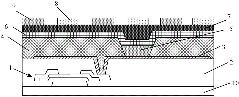
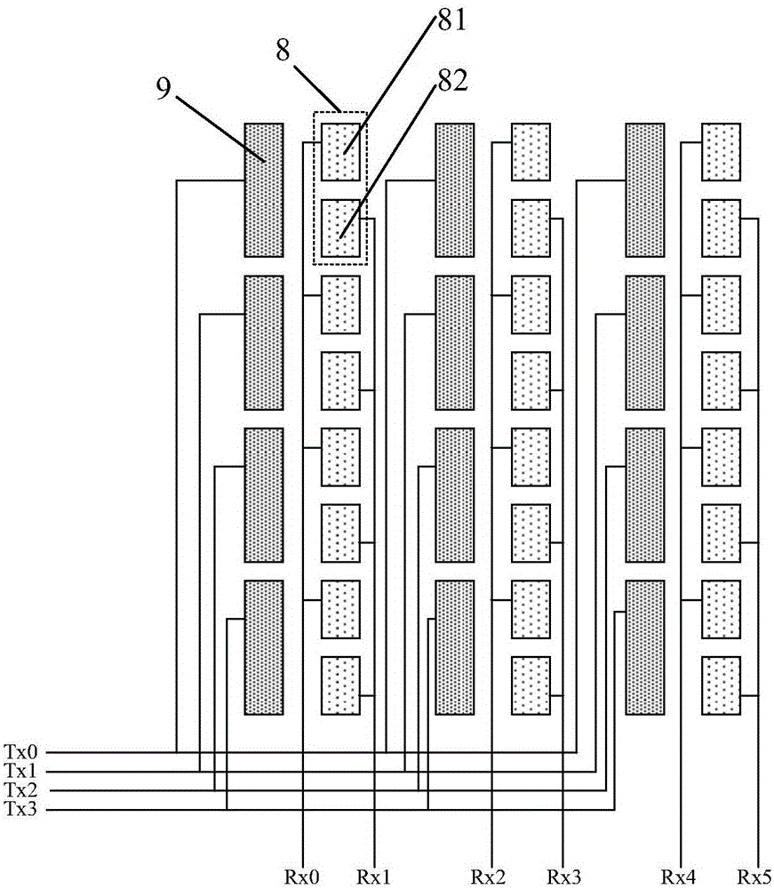
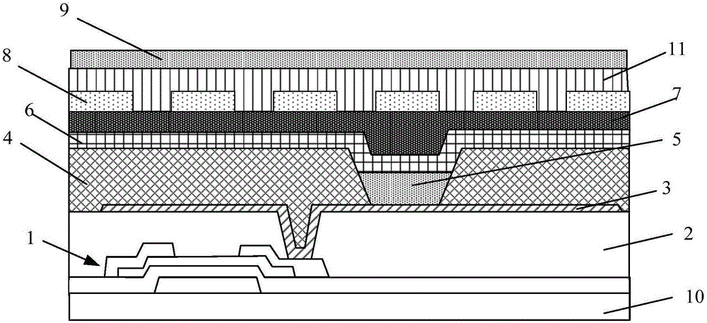
[0037] Such as Figures 1 to 3 As shown, this embodiment provides a touch panel, which includes an OLED substrate facing each other and a substrate facing each other; the OLED substrate includes at least a substrate 10, and a plurality of organic electroluminescent devices arranged above the substrate 10; The organic electroluminescent device includes a first electrode 3, a light-emitting layer 5, and a second electrode 6 sequentially arranged above the substrate 10, and the touch panel also includes an electrode arranged on the light-emitting surface side of the second electrode 6, and The second electrode 6 is a touch electrode and a sensing electrode arranged in isolation.

[0038] Since the touch electrodes and sensing electrodes of the touch panel of this embodiment are arranged on the second electrode 6 of the organic electroluminescence device, and are insulated from the second electrode 6, that is to say, the touch electrodes and the The sensing electrodes are layered...

Embodiment 2

[0051] Such as Figure 4 As shown, this embodiment provides a method for preparing a touch panel, and the method is used to prepare the touch panel described in Embodiment 1. Wherein, the first electrode 3 is an anode, and the second electrode 6 is a cathode as an example to describe the preparation method of this embodiment. The preparation method specifically includes:

[0052] Step 1, forming various layer structures including the thin film transistor 1 on the substrate 10, then forming the passivation layer 2, and etching the passivation layer 2 to form a pass for connecting the drain of the thin film transistor 1 to the anode of the organic electroluminescent device hole.

[0053] Step 2. On the substrate 10 that has completed the above steps, a pattern including the anode of the electroluminescent device is formed through a patterning process; then a pixel defining layer 4 is formed, and a luminescent material is formed in the pixel defining layer 4 to form an electrol...

Embodiment 3

[0060] Such as Figure 5 As shown, this embodiment provides a method for preparing a touch panel, and the method is used to prepare the touch panel described in Embodiment 1. Wherein, the first electrode 3 is an anode, and the second electrode 6 is a cathode as an example to describe the preparation method of this embodiment. The preparation method specifically includes:

[0061] Step 1, forming various layer structures including the thin film transistor 1 on the substrate 10, then forming the passivation layer 2, and etching the passivation layer 2 to form a pass for connecting the drain of the thin film transistor 1 to the anode of the organic electroluminescent device hole.

[0062] Step 2. On the substrate 10 that has completed the above steps, a pattern including the anode of the electroluminescent device is formed through a patterning process; then a pixel defining layer 4 is formed, and a luminescent material is formed in the pixel defining layer 4 to form an electrol...


PUM


Abstract

The invention provides a touch control panel, a preparing method of the touch control panel and a display device, and belongs to the technical field of display. The problem of influence of a touch control electrode and a sensing electrode in the existing touch control panel on the illumination of organic electroluminescence devices can be solved. The touch control panel comprises an OLED (Optical Light Emitting Device) base plate and a matched base plate which match with each other, wherein the OLED base plate at least comprises a substrate and a plurality of organic electroluminescence devices arranged on the substrate; each organic electroluminescence device comprises a first electrode, a luminous layer and a second electrode which are sequentially arranged on the substrate; the touch control panel also comprises a touch control electrode and a sensing electrode; and the touch control electrode and the sensing electrode are arranged at the emergent surface side of the second electrode and are arranged in a way of being isolated from the second electrode.

Description

technical field [0001] The invention belongs to the field of display technology, and in particular relates to a touch panel, a preparation method thereof, and a display device. Background technique [0002] Compared with liquid crystal displays, organic light-emitting diode (Organic Light-emitting Devices, OLED) displays have advantages such as fast response speed, light weight, bendability and wide viewing angle. [0003] The OLED display panel is the main component of the OLED display. Wherein, the OLED display panel includes an OLED substrate and a cell-aligned substrate facing each other. The display panel with touch function is the main product in the display field today. Among them, the multi-capacitance full in-cell touch (Muliti-capacitancefullincellTouch) OLED display panel has become the research focus of touch technology in recent years due to its simple structure and cost advantages. The touch electrodes and sensing electrodes of the display panel are arranged...

Claims


Application Information

Patent Timeline
Patent Type & Authority Applications(China)
IPC IPC(8): G06F3/041
CPCG06F2203/04103G06F3/0443G06F3/0446G06F3/04164H10K59/40
Inventor 许睿陈小川王磊杨盛际刘英明蔡佩芝王海生
Owner BOE TECH GRP CO LTD
Why Eureka
Try Eureka