Laser marking device of semiconductor chip

A technology of laser marking and laser marking machine, which is applied in the direction of semiconductor devices, laser welding equipment, circuits, etc. The effect of controllable range, reduced photographic field of view, and reduced cost

Inactive Publication Date: 2015-12-23
BEIJING CHN TOP OPTICAL ELECTRONICS TECH
View PDF8 Cites 2 Cited by
  • Summary
  • Abstract
  • Description
  • Claims
  • Application Information

AI Technical Summary

Problems solved by technology

Make a positive film for each semiconductor wafer, so that each semiconductor wafer is at the same position and angle during marking. The structure of the positive film machine used is complex. In actual operation, the positive film of a semiconductor wafer needs to be transported by a robot many times. , which takes a long time and affects the laser marking efficiency of semiconductor wafers

Method used


Image

  • Laser marking device of semiconductor chip
  • Laser marking device of semiconductor chip
  • Laser marking device of semiconductor chip

Examples


Embodiment 1

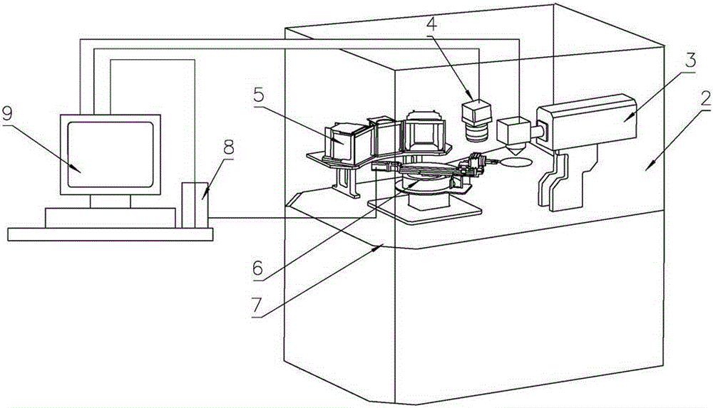
[0014] Depend on figure 2 Schematically, the present invention mainly includes: a frame 7, a marking room 2, a laser marking machine 3, a manipulator movement mechanism 6, a bin mechanism 5, a computer 9, and a motion controller 8, wherein the laser marking machine 3 passes through a control line The cable is connected to the computer 9, the camera 4 is connected to the computer 9 through the control cable, the manipulator movement mechanism 6 is connected to the motion controller 8 through the control cable, the computer 9 is connected to the motion controller 8 through the control cable, and the laser Marking machine 3, camera 4, manipulator movement mechanism 6 and silo mechanism 5 are all fixed on frame 7, and laser marking machine 3, camera 4, manipulator movement mechanism 6 and hopper mechanism 5 are placed in marking room 2 Inside, the laser marking machine 3 is located above the highest movement position of the mechanical arm in the manipulator movement mechanism 6, ...

Embodiment 2

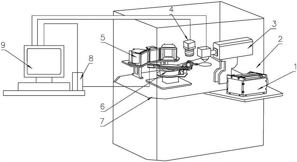
[0017] like image 3 Schematically, the difference between this embodiment and Embodiment 1 is that a leveler 1 is installed, the leveler 1 is fixed on the frame 7, and placed outside the marking room 2, and the others are the same as in Embodiment 1.

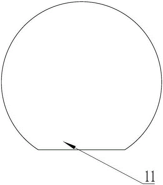
[0018]The leveler 1 is used to positively film a box of semiconductor wafers. When in use, the magazine containing the semiconductor wafers is placed on the leveler 1 on the mounting surface on the same side as the rotating roller, and semiconductor wafers 11 of different sizes The mounting surface on which the box is placed is also different. Through the rotation of the rotating roller on the leveler 1, when the short flat chord side of the semiconductor wafer in the magazine is tangent to the rotating roller, the semiconductor wafer in the magazine is in a static state and is ready to be processed. When all the semiconductor wafers in the box were at rest, the short flat chord sides of the semiconductor wafers 11 in the mag...


PUM


Abstract

The invention relates to a laser marking device, especially relates to a laser marking device of a semiconductor chip. The laser marking device mainly comprises a frame (7), a marking chamber (2), a laser marking machine (3), a manipulator motion mechanism (6), a bin mechanism (5), a calculator (9), and a motion controller (8), wherein the laser marking machine (3) is connected with the calculator (9) by a control cable, the manipulator motion mechanism (6) is connected with the motion controller (8) by the control cable, the calculator (9) is connected with the motion controller (8) by the control cable. The laser marking device also comprises a camera (4) connected with the calculator (9) by the control cable, so that a picture of the profile of the semiconductor chip in need of marking can be took by the camera, and the profile data can be calculated and analyzed by the calculator, and the semiconductor chip is subjected to laser marking by the laser marking device according to the motion direction of calculation.

Description

technical field [0001] The invention relates to a laser marking device, in particular to a laser marking device for a semiconductor wafer. Background technique [0002] When semiconductor wafer manufacturers distinguish different semiconductor wafers of the same shape, they need to number each semiconductor wafer and etch the corresponding number on the semiconductor wafer. Generally, lasers are used to irradiate the position of the semiconductor wafer that needs to be marked. Ablation completes the number etching of the semiconductor wafer. Usually the size of the semiconductor wafer is 2 inches to 6 inches. The semiconductor wafer is a circle with the short flat chord side removed. The semiconductor wafer manufacturer will etch the corresponding number on the short flat chord side. , in order to ensure the consistency of the numbering positions of different semiconductor wafers of the same size, when etching the numbers of different semiconductor wafers of the same size ea...

Claims


Application Information

Patent Timeline
Patent Type & Authority Applications(China)
IPC IPC(8): B23K26/362B23K26/70B23K101/40
Inventor 郭金源伊文君徐杰
Owner BEIJING CHN TOP OPTICAL ELECTRONICS TECH
Why Eureka
Try Eureka