Organic electroluminescent device, manufacturing method thereof and display device

An electroluminescent device and electroluminescent technology, applied in the manufacturing of organic semiconductor devices, electro-solid devices, semiconductor/solid-state devices, etc., can solve the problems of reducing luminous efficiency, not effectively improving, affecting OLED performance, etc. Effect of Luminous Efficiency

Inactive Publication Date: 2015-12-23
BOE TECH GRP CO LTD
View PDF2 Cites 2 Cited by
  • Summary
  • Abstract
  • Description
  • Claims
  • Application Information

AI Technical Summary

Problems solved by technology

[0003] In an existing OLED device, a blue light-emitting layer, a red light-emitting layer or a green light-emitting layer is included, the blue light-emitting layer is adjacent to the red and / or green light-emitting layer, and the blue light-emitting layer is adjacent to the red and / or green light-emitting layer. New luminescent species are generated between the green light-emitting layers, which reduces the luminous efficiency
And the existing OLEDs have not effectively improved this, which will inevitably affect the performance of OLEDs

Method used


Image

  • Organic electroluminescent device, manufacturing method thereof and display device
  • Organic electroluminescent device, manufacturing method thereof and display device
  • Organic electroluminescent device, manufacturing method thereof and display device

Examples


Embodiment 1

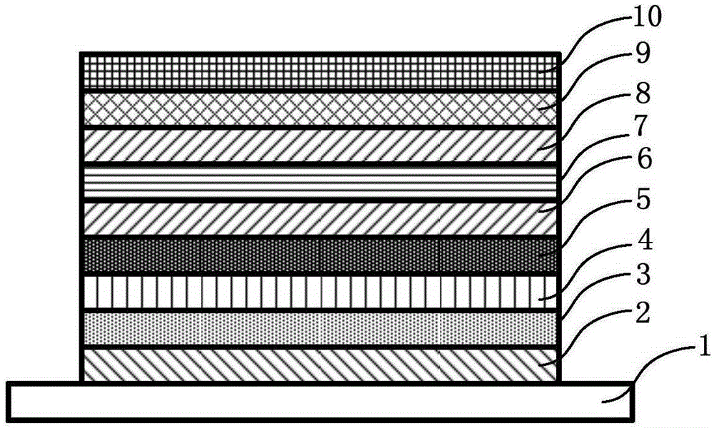
[0059] In order to more clearly illustrate the technical solution of the present invention, the following combination image 3 The cross-sectional schematic diagram of the structure of the organic electroluminescent device shown in the illustrated embodiment 1, as Figure 4 As shown, the manufacturing method of this embodiment may specifically include the following steps:

[0060] S1: forming an indium tin oxide (Indium Tin Oxides, ITO) layer on the substrate 1, and etching the ITO layer to form the first electrode 2;

[0061] Wherein, the substrate 1 is transparent glass, and the thickness of the first electrode 2 is about 70 nm. It should be noted that after the first electrode 2 is formed, the ITO glass substrate is cleaned in an ultrasonic environment of deionized water, acetone and absolute ethanol, and then dried with nitrogen N2 and treated with oxygen plasma.

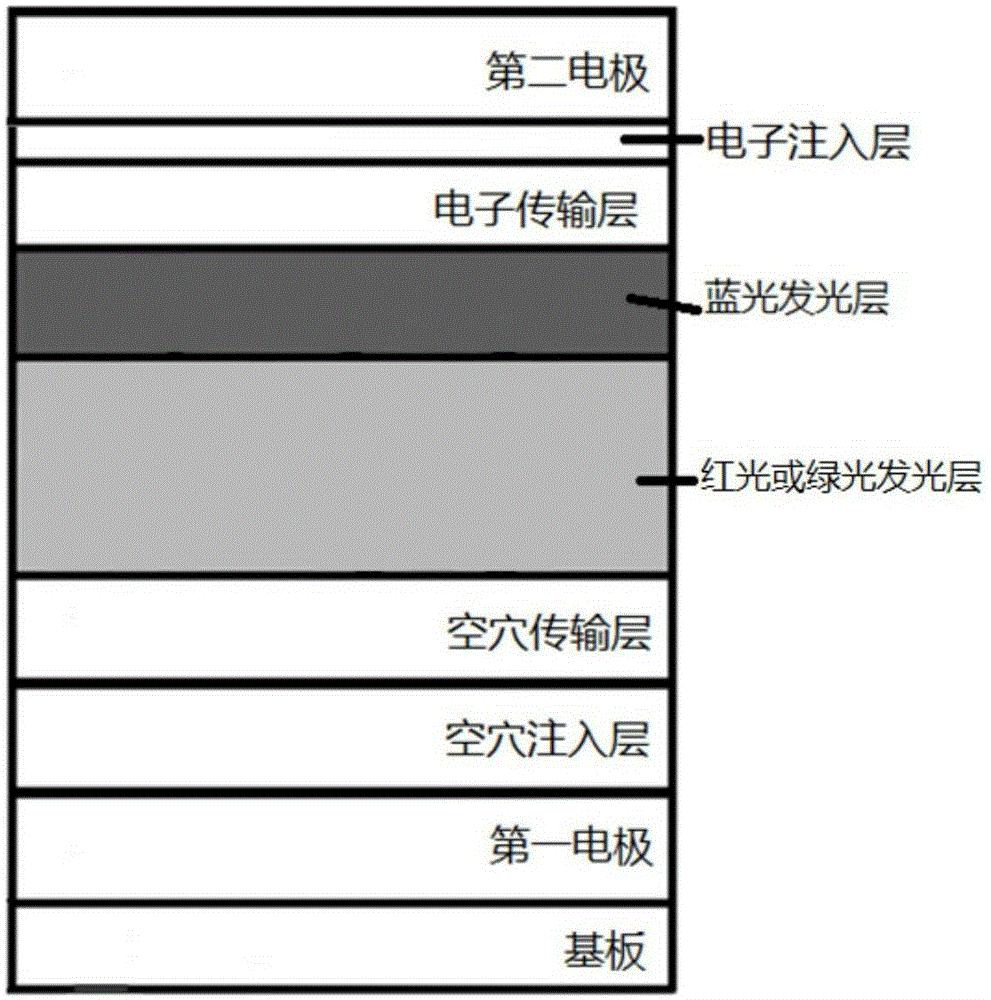
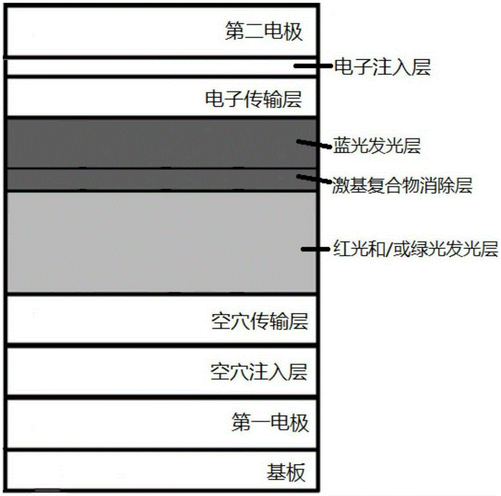
[0062] S2: The hole injection layer 3, the hole transport layer 4 and the green light emitting layer 5 are sequentia...


PUM


Abstract

The present invention provides an organic electroluminescent device which comprises a substrate, a first electrode, a red and/or green light emitting layer, a blue light emitting layer, a second electrode, and an exciplex elimination layer formed between the red and/or green light emitting layer and the blue light emitting layer, wherein the exciplex elimination layer allows carriers to be limited in the red and/or green light emitting layer. The invention also provides the above organic electroluminescent device. According to the organic electroluminescent device, the manufacturing method thereof and the display device, the carriers are allowed to be limited in the red and/or green light emitting layer, the composition of the carriers in the red and/or green light emitting layer is ensured and red light and/or green light is emitted, and the light emitting efficiency is improved.

Description

Technical field [0001] The invention relates to the technical field of semiconductor preparation, in particular to an organic electroluminescent device, a manufacturing method thereof, and a display device. Background technique [0002] An organic electroluminescence display device (Organic Light Emitting Diode, OLED) is a display device that electrically excites phosphors or phosphor organic compounds to emit light. Organic electroluminescent devices (OLED) are considered to have huge application prospects in flat panel displays because of their self-luminous, all-solid-state, wide viewing angle, fast response and many other advantages, after liquid crystal (LCD) and plasma (PDP) A new generation of flat panel display products. In order to ensure that the OLED device has higher functional reliability and lower energy consumption, it is necessary to improve the luminous efficiency of the OLED device as much as possible. [0003] Existing OLED devices include a blue light emitting...

Claims


Application Information

Patent Timeline
Patent Type & Authority Applications(China)
IPC IPC(8): H01L51/50H01L51/56
CPCH10K30/865H10K71/00H10K71/12H10K71/164H10K85/115H10K85/1135H10K85/611H10K85/631H10K85/6572H10K85/342H10K50/11H10K2101/40H10K50/131H10K2101/30H10K85/111
Inventor 廖金龙
Owner BOE TECH GRP CO LTD
Why Eureka
Try Eureka