Gate driving circuit and driving method thereof as well as display device

A gate drive circuit and drive method technology, applied in static indicators, instruments, etc., can solve the problems of received signal strength attenuation, signal delay, etc.

Active Publication Date: 2015-12-30
BOE TECH GRP CO LTD +1
View PDF4 Cites 14 Cited by
  • Summary
  • Abstract
  • Description
  • Claims
  • Application Information

AI Technical Summary

Problems solved by technology

[0006] Embodiments of the present invention provide a gate drive circuit, its drive method, and a display device, which ca

Method used


Image

  • Gate driving circuit and driving method thereof as well as display device
  • Gate driving circuit and driving method thereof as well as display device
  • Gate driving circuit and driving method thereof as well as display device

Examples


Embodiment 1

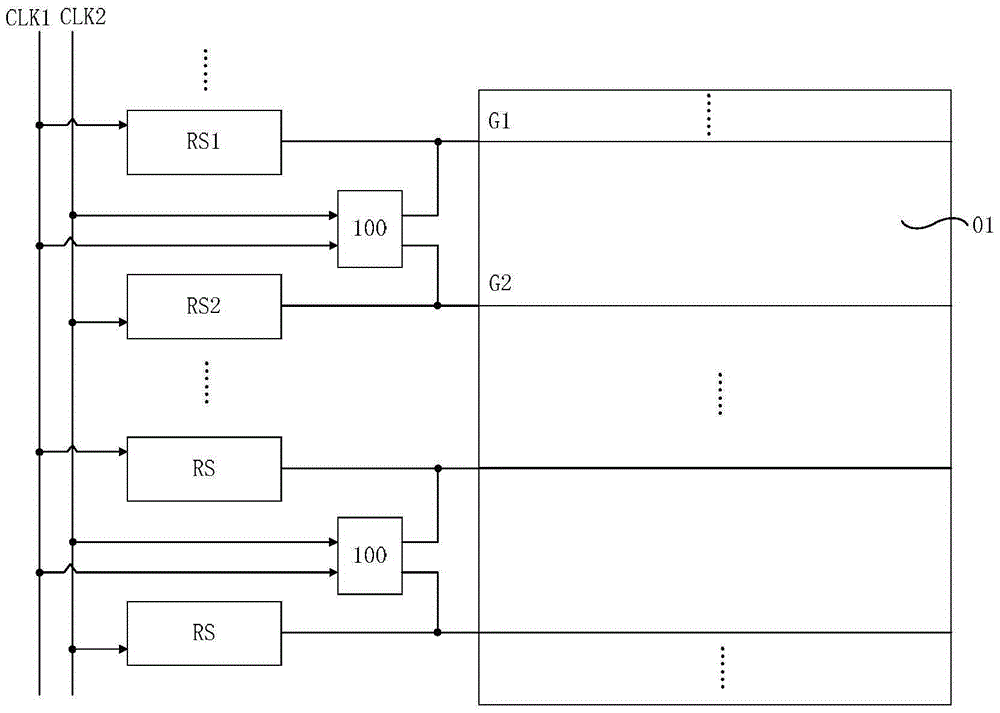
[0061] The structure of the pre-charging unit 100 in this embodiment is as follows Image 6 As shown, it includes a first transistor T1, a second transistor T2 and a third transistor T3.

[0062] Wherein, the gate and the first pole of the first transistor T1 are connected to the second clock signal terminal CLK2, and the second pole is connected to the gate of the second transistor T2.

[0063] The first pole of the second transistor T2 is connected to the first gate line G1, and the second pole is connected to the gate of the third transistor T3.

[0064] A first pole of the third transistor T3 is connected to the first clock signal terminal CLK1, and a second pole is connected to the second gate line G3.

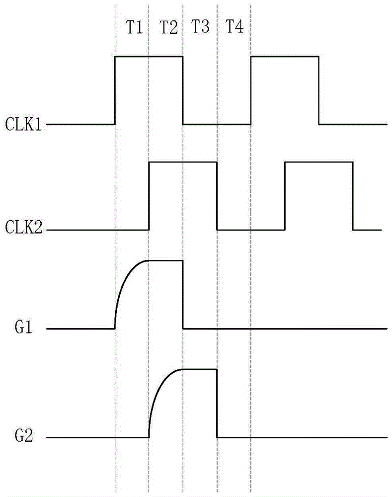
[0065] In this way, if figure 2 As shown, at the second moment T2, the second clock signal terminal CLK2 outputs a high level, which turns on the first transistor T1, so that the second clock signal terminal CLK2 outputs a high level through the first transistor T1 to ...

Embodiment 2

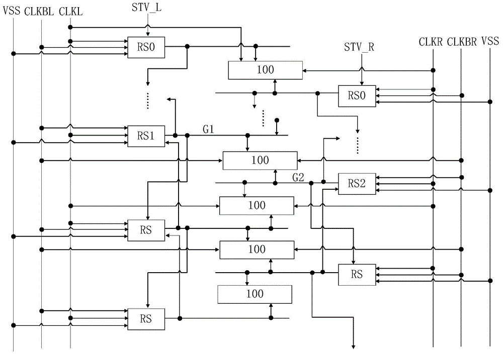
[0067] The structure of the pre-charging unit 100 in this embodiment is as follows Figure 7 As shown, it can be seen that the pre-charging unit 100 in this embodiment includes all the transistors in the first embodiment (namely, the first transistor T1, the second transistor T2 and the third transistor T3), and in addition, the pre-charging unit 100 also includes The fourth transistor, and the pre-charging unit 100 is connected to the start signal terminal STV.

[0068] Wherein, the gate of the fourth transistor is connected to the start signal terminal STV, the first pole is connected to the gate of the second transistor T2, and the second pole is connected to the reset voltage terminal VSS. Wherein, the reset voltage terminal VSS can generally be input with a low level or be grounded. In this way, when the pre-charging unit 100 performs the pre-charging action, the fourth transistor T4 can be used to Figure 7 Reset the potential at the node PU in order to prevent the res...


PUM


Abstract

The embodiment of the invention provides a gate driving circuit and a driving method thereof as well as a display device, relates to the technical field of displaying and can solve the problems of signal receiving strength reduction and signal delay of pixel units farther from shift registers. The gate driving circuit is used for driving at least two adjacent gate lines, namely a first gate line and a second gate line on a display panel; the gate driving circuit at least comprises a first shift register unit, a second shift register unit and a precharge unit; the precharge unit is connected with the first gate line, the second gate line, a first clock signal terminal and a second clock signal terminal, and used for outputting signals of the first clock signal terminal to the second gate line under the control of the second clock signal terminal and the first gate line; the rising edge of output signals of the second clock signal terminal is positioned between the rising edge and the failing edge of the output signals of the first clock signal terminal or the falling edge of the second clock signal terminal is positioned between the rising edge and the falling edge of the output signals of the first clock signal terminal.

Description

technical field [0001] The present invention relates to the field of display technology, in particular to a gate driving circuit, a driving method thereof, and a display device. Background technique [0002] In the process of making a Liquid Crystal Display (LCD for short) or an Organic Light-Emitting Diode (OLED for short) display, it is necessary to manufacture a driver IC (Integrated Circuit, integrated circuit) on the non-conductive part of the display panel through a bonding process. display area to input a driving signal to the display panel. [0003] In order to reduce costs, GOA (GateDriveronArray, array substrate row drive) technology is used in the prior art to integrate TFT (ThinFilmTransistor, thin film field effect transistor) gate switch circuits on the array substrate of the display panel to form a scan drive for the display panel. Thereby, the part of the gate driver IC can be saved. [0004] In the process of display driving, the GOA circuit sequentially s...

Claims


Application Information

Patent Timeline
IPC IPC(8): G09G3/36G09G3/32
Inventor 王俊伟封宾
Owner BOE TECH GRP CO LTD
Why Eureka
Try Eureka