Semiconductor device and manufacturing method thereof, and electronic apparatus

A manufacturing method and semiconductor technology, which are applied in the fields of semiconductor devices, semiconductor/solid-state device manufacturing, electric solid-state devices, etc., can solve the conflict between the writability and reading stability of SRAM cells, and improve the writability and readability. The effect of stability

Active Publication Date: 2015-12-30
SEMICON MFG INT (SHANGHAI) CORP
View PDF6 Cites 3 Cited by
  • Summary
  • Abstract
  • Description
  • Claims
  • Application Information

AI Technical Summary

Problems solved by technology

Therefore, the different requirements on the performance of the pass transistors create a conflict between the writeability and read stability of the SRAM cell
And this conflict has always been the bottleneck of traditional 6TSRAM memory cell design

Method used


Image

  • Semiconductor device and manufacturing method thereof, and electronic apparatus
  • Semiconductor device and manufacturing method thereof, and electronic apparatus
  • Semiconductor device and manufacturing method thereof, and electronic apparatus

Examples


Embodiment 1

[0041] Below, refer to Figure 3A-3B , Figure 4 and Figures 5A-5B The manufacturing method of the semiconductor device according to the embodiment of the present invention is described in detail.

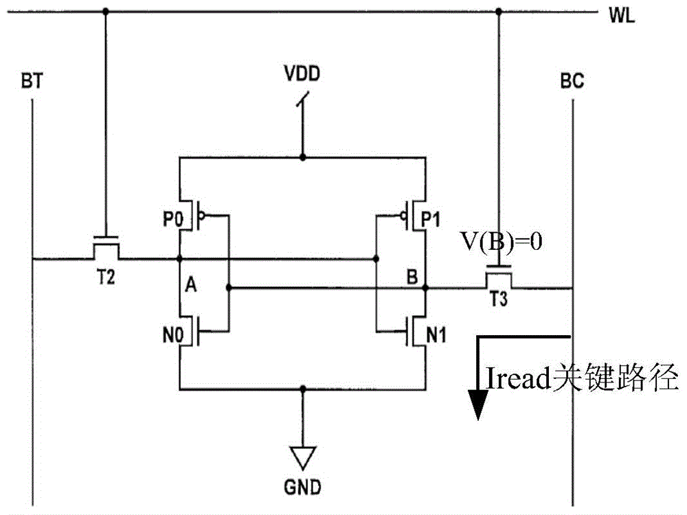
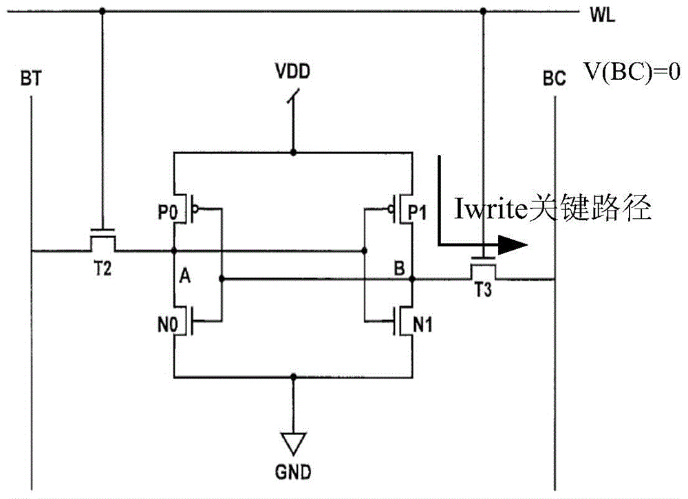
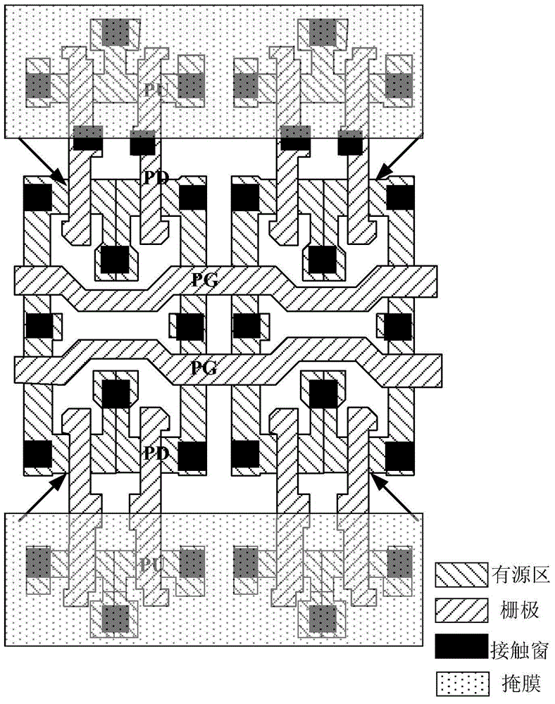
[0042] refer to Figure 4 , performing step 401, providing a semiconductor substrate, on which a front-end device of a plurality of storage units is formed, the storage unit includes at least two pull-up transistors formed on the semiconductor substrate, at least two pull-down transistors and at least two pass-gate transistors, wherein each of the pull-up transistors, the pull-down transistors, and the pass-gate transistors includes a gate and gate sidewalls.

[0043] Specifically, refer to Figure 3A , is a top view of a plurality of storage units formed according to an embodiment of the present invention, taking one of the storage units as an example.

[0044] A semiconductor substrate is provided, and the semiconductor substrate can be at least one of the materials mention...

Embodiment 2

[0060] Embodiment 2 of the present invention provides a semiconductor device, which can be manufactured by using the manufacturing method of the semiconductor device in Embodiment 1 above.

[0061] The semiconductor device of this embodiment includes a plurality of storage units, and the storage units include at least two pull-up transistors, at least two pull-down transistors, and at least two pass-gate transistors, wherein, in each of the storage units, the The two pass-gate transistors have asymmetric pocket regions with different doping concentrations.

[0062] Wherein, for example, the pocket region located between the gates of the two adjacent pass-gate transistors is a highly doped pocket region, and the pocket region located outside the two pass-gate transistors is a highly doped pocket region.

[0063] Wherein, the semiconductor device is a static random access memory.

[0064] In the semiconductor device of the embodiment of the present invention, due to the transmi...

Embodiment 3

[0066] An embodiment of the present invention provides an electronic device using the semiconductor device manufactured according to the method for manufacturing a semiconductor device described in Embodiment 1, or using the semiconductor device described in Embodiment 2. The electronic device has better performance due to the semiconductor devices used having different device ratios.

[0067] The electronic device may be any electronic product or device such as a mobile phone, a tablet computer, a notebook computer, a netbook, a game console, a TV set, a VCD, a DVD, a navigator, a camera, a video camera, a voice recorder, MP3, MP4, or PSP.


PUM


Abstract

The invention provides a semiconductor device and a manufacturing method thereof, and an electronic apparatus. The manufacturing method includes: a semiconductor substrate is provided, front devices of a plurality of memory cells are formed on the semiconductor substrate, each memory cell comprises at least two pull-up transistors, at least two pull-down transistors, and at least two pass-gate transistors, wherein the pull-up transistors, the pull-down transistors, and the pass-gate transistors all comprise grid electrodes and grid electrode sidewalls, and asymmetric pocket ion implantation is performed for the two pass-gate transistors of each memory cell. According to the manufacturing method for the semiconductor device, the pass-gate transistors in asymmetric pocket areas with different doping concentrations are formed, the conflict between the writability and the reading stability of an SRAM unit can be effectively balanced, the writability and the reading stability of the SRAM unit are improved, and the reliability of the SRAM unit is improved.

Description

technical field [0001] The invention relates to the technical field of semiconductor storage, in particular to a semiconductor device, a manufacturing method thereof, and an electronic device. Background technique [0002] With the continuous development of digital integrated circuits, on-chip integrated memory has become an important part of digital systems. SRAM (StaticRandomAccessMemory, static random access memory) has become an indispensable and important part of the on-chip memory with its advantages of low power consumption and high speed. SRAM can hold data as long as it is powered, there is no need to constantly refresh it. [0003] The basic SRAM storage unit generally includes six transistors: 2 pull-up transistors PU (Pull-up transistor), 2 pull-down transistors PD (Pull-down transistor), and 2 pass-gate transistors PG (Pass-gate transistor). In the design process of SRAM memory cells, it is usually necessary to ensure a sufficiently large β ratio (Ipd / Ipg curr...

Claims


Application Information

Patent Timeline
Patent Type & Authority Applications(China)
IPC IPC(8): H01L21/8244H01L27/11
Inventor 王楠王颖倩李煜王媛
Owner SEMICON MFG INT (SHANGHAI) CORP
Why Eureka
Try Eureka