Bidirectional transient voltage suppressing diode and manufacturing method thereof

A technology of transient voltage suppression and manufacturing method, which is applied in the direction of semiconductor/solid-state device manufacturing, circuits, electrical components, etc., can solve the problems of protection circuit burnout, large deviation and asymmetry of suppressed voltage and surge current, etc. Current capability, does not affect the effect of the package

Active Publication Date: 2015-12-30
BYD SEMICON CO LTD
View PDF5 Cites 9 Cited by
  • Summary
  • Abstract
  • Description
  • Claims
  • Application Information

AI Technical Summary

Problems solved by technology

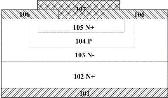
[0004] The transient voltage suppression diode formed by this process is due to the asymmetry of the PN junction formed by the N- epitaxial layer 103 and the P well region 104 and the PN junction area and structure formed by the P well region 104 and the N+ active region 105 (P well region PN junction area formed by 104 and N+ active region 105 is always smaller than the PN junction area formed by N- epitaxial layer 103 and P well region 104, and is surrounded by the PN junction formed by P well region 104 and N+ active region 105), resulting in this The asymmetry of the positive and negative suppression voltage and surge current of the device makes the device work in the forward and reverse directions. One-way burning of the circuit occurs

Method used


Image

  • Bidirectional transient voltage suppressing diode and manufacturing method thereof
  • Bidirectional transient voltage suppressing diode and manufacturing method thereof
  • Bidirectional transient voltage suppressing diode and manufacturing method thereof

Examples


Embodiment Construction

[0021] Embodiments of the present invention are described in detail below, examples of which are shown in the drawings, wherein the same or similar reference numerals designate the same or similar elements or elements having the same or similar functions throughout. The embodiments described below by referring to the figures are exemplary only for explaining the present invention and should not be construed as limiting the present invention.

[0022] In describing the present invention, it should be understood that the terms "longitudinal", "transverse", "upper", "lower", "front", "rear", "left", "right", "vertical", The orientation or positional relationship indicated by "horizontal", "top", "bottom", "inner", "outer", "front", "back", etc. are based on the orientation or positional relationship shown in the attached drawings, and are only for the convenience of description The present invention and simplified description do not indicate or imply that the device or element re...


PUM


Abstract

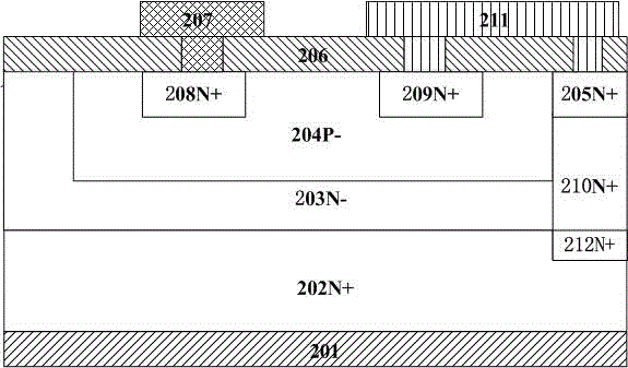
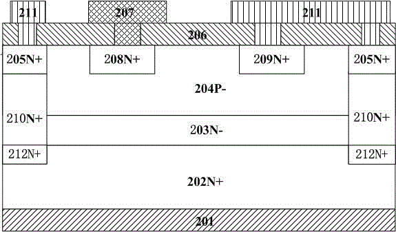
The invention provides a bidirectional transient voltage suppressing diode and a manufacturing method thereof. A second active region and a third active region, which are simultaneously formed and are of the same conductivity type, doped concentration and shape, are arranged in the diode. The longitudinal NPN or PNP structure of a traditional bidirectional transient voltage suppressing diode is changed into a transverse NPN or PNP structure. Via a current channel formed by a conducting layer, a buried layer and a first active region, symmetrical forward and backward suppressing voltage is ensured no matter whether forward voltage or backward voltage is applied to the diode. The whole diode is of a longitudinal structure, and the current carrying capacity of the diode is ensured without influencing encapsulation.

Description

technical field [0001] The invention belongs to the field of basic electrical components and relates to the preparation of semiconductor devices, in particular to a bidirectional transient voltage suppression diode and a manufacturing method thereof. Background technique [0002] Transient Voltage Suppressor Diode (TVS for short) is a PN junction semiconductor diode device formed by silicon diffusion process. When the two poles of TVS are impacted by the reverse transient high energy, it can change the high impedance between the two poles to low impedance in 10-12s order to absorb the surge power up to several thousand watts, so that the two poles The voltage is clamped at a predetermined value, which effectively protects the precision components in the electronic circuit from being damaged by various surge pulses and static electricity. There are two types of TVS: Unidirectional TVS and Bi-directional TVS. The bidirectional TVS is equivalent to two unidirectional TVS conn...

Claims


Application Information

Patent Timeline
Patent Type & Authority Applications(China)
IPC IPC(8): H01L29/861H01L29/06H01L21/329
Inventor 王艳春
Owner BYD SEMICON CO LTD
Why Eureka
Try Eureka