High-speed differential dual-modulus prescaler

A high-speed differential and prescaler technology, applied in the direction of automatic power control, electrical components, etc., can solve the problems of low power consumption, unsuitable for dual-mode prescaler, low clock frequency requirements, etc.

Active Publication Date: 2015-12-30
SHANGHAI SIFLOWER COMM TECH CO LTD
View PDF3 Cites 0 Cited by
  • Summary
  • Abstract
  • Description
  • Claims
  • Application Information

AI Technical Summary

Problems solved by technology

[0003] Today, high-speed dual-mode prescalers have been developed, the first being a standard-based digital flip-flop circuit with the obvious disadvantage of being the slowest
The second is based on differential current-mode logic (CML), which is much faster than the first but consumes a lot of power
But since each dynamic flip-flop has a minimum clock frequency requirement, it is not suitable for dual-mode prescaler
The fourth is a dynamic circuit based on an inverter with clock enable and an AND-OR logic gate, which also has the defect that each dynamic flip-flop has a minimum clock frequency requirement
[0004] Therefore, designing a high-speed differential dual-mode prescaler with fast trigger speed, low power consumption and suitable for dual-mode prescaler has become a major problem faced by those skilled in the art.

Method used


Image

  • High-speed differential dual-modulus prescaler
  • High-speed differential dual-modulus prescaler
  • High-speed differential dual-modulus prescaler

Examples


Embodiment 1

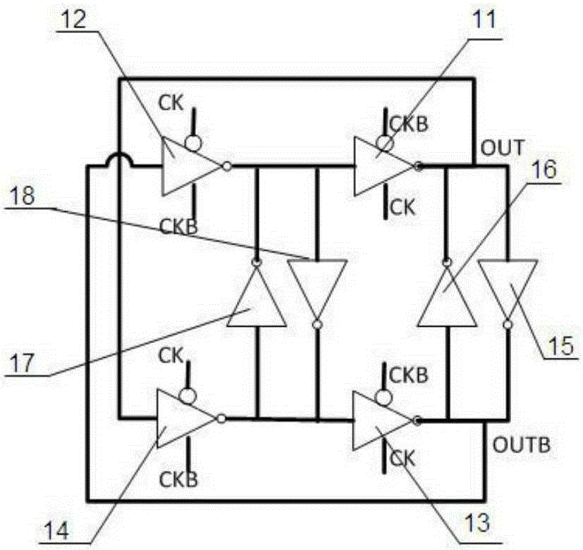
[0075] see Figure 4 The structure shown is a circuit diagram of a radio frequency divider by 2 / 3 frequency divider in an embodiment of the present invention, which includes a first-stage reverse circuit, a second-stage reverse circuit, a third-stage reverse circuit and a fourth-stage reverse circuit. Inverting circuit, wherein, the first-stage inverting circuit includes the first clock-enabled NAND circuit 413 and the first clock-enabled NOR gate circuit 49, and the second-stage inverting circuit includes the first band clock-enabled NOR gate circuit 49. Phaser 414 and the second band clock enable inverter 410, the input end of its first band clock enabling inverter 414 is connected with the output end of the first NAND gate circuit 413, and the second band clock enables inverting The input end of the device 410 is connected with the output end of the first band clock enabling NOR gate circuit 49; the third stage reverse circuit includes the second band clock enabling NAND ga...

specific Embodiment 1

[0076] Input a high-level signal "1" to the first input terminal and the second input terminal of the first clock-enabled NAND gate circuit respectively, then the output terminal of the first clock-enabled NAND gate circuit outputs a low-level signal "0", then the first band clock enables the inverter 414 to output a signal "1", and the signal "1" is transmitted to the first input terminal ① of the second band clock enabling AND-OR gate circuit 415 while also transmitting To the first input terminal ① of the first NOR gate circuit 49, preferably the second input terminal input signal "1" of the second band clock enabling the AND gate circuit 415, the second band clock enabling the AND gate circuit 415 Output signal "0", this signal is transmitted to the input end of the third belt clock enabling inverter 416, then the third belt clock enabling inverter 416 outputs a signal "0", this signal "0" is also used as the first The input signal of the second input terminal of the one-N...

Embodiment 2

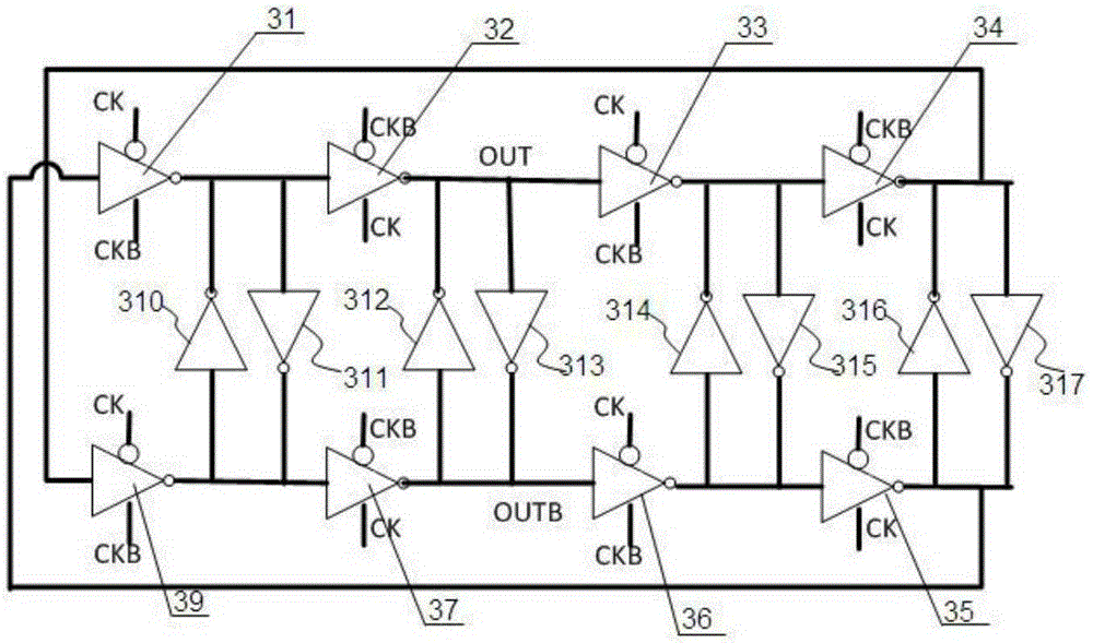
[0083] see Figure 6 As shown in the structure, the present invention provides a frequency divider divided by 3 / 4 frequency divider circuit, the frequency divider circuit includes a logic gate circuit, a first stage inverting circuit, a second stage inverting circuit, a third stage inverting circuit circuit and the fourth stage reverse circuit, wherein, the logic gate circuit includes the OR gate circuit 517 and the AND gate circuit 50, the first stage reverse current circuit includes the NAND gate circuit 516 and the NOR gate circuit 59, and the second stage reverse current circuit Including the first clock-enabled inverter 515 and the second clock-enabled inverter 510, the third reverse current includes the third band clock-enabled inverter 514 and the fourth band clock-enabled inverter 511, the fourth stage of reverse current includes a fifth inverter with clock enabling 513 and a sixth inverter with clock enabling 512, wherein a reverse circuit of the first stage and the r...


PUM


Abstract

The invention belongs to the technical field of radio frequency communication chips, and particularly relates to a high-speed differential dual-modulus prescaler which is used for a multi-GHz frequency comprehensive phase-locked loop design technology. According to the high-speed differential dual-modulus prescaler, a logic gate of a trigger input end is combined with input-stage clock enable inverters, and a logic gate conversion rule that input and output are in inverse relationships is utilized. By means of latches between differential circuits, high-speed dynamic circuits are converted to high-speed static steady-state circuits. According to the technical scheme, a high-speed and low-power dual-modulus prescaler design technology which is suitable for a novel deep submicron process is provided, and the design requirement of frequency division of a frequency synthesizer and a local oscillator in a wireless radio frequency communication chip at present is effectively met.

Description

technical field [0001] The invention belongs to the technical field of radio frequency communication chips, and can be used for multi-GHz (multi-GHz) frequency synthesis phase-locked loop design technology, in particular to a high-speed differential dual-mode prescaler. Background technique [0002] With the advancement of wireless communication technology and semiconductor technology, the design requirements of wireless communication chips are also getting higher and higher. The trends of high performance, low power consumption, high integration and low cost dominate the evolution of chip design technology. RF frequency synthesizer (RFfrequencysynthesizer) is a mixer (mixer) used for conversion between baseband signals and radio frequency signals, and is a key module in RF Transceiver (RFTransceiver). The high-speed dual-mode prescaler (high-speeddual-modulusprescaler) connected to the voltage-controlled oscillator (VCO) is still the speed bottleneck of the frequency synth...

Claims


Application Information

Patent Timeline
Patent Type & Authority Applications(China)
IPC IPC(8): H03L7/18
Inventor 束克留李兴仁石亚飞
Owner SHANGHAI SIFLOWER COMM TECH CO LTD
Why Eureka
Try Eureka