Preparation method of planar TEM sample

A sample and plane technology, applied in the field of preparation of TEM plane samples, can solve the problems of poor TEM imaging effect, inability to carry out analysis work, influence, etc., and achieve the effect of improving quality and success rate

Active Publication Date: 2016-01-06
SHANGHAI HUALI MICROELECTRONICS CORP
View PDF4 Cites 4 Cited by
  • Summary
  • Abstract
  • Description
  • Claims
  • Application Information

AI Technical Summary

Problems solved by technology

[0008] However, in the sample preparation method of the prior art, the first cutting plane is usually located at the position of the poly layer, so the TEM observation will be affected by the masking of the lattice image on the polycrystalline poly
As we all know, the ability of TEM high-resolution observation is through electron penetration imaging. Since Poly is a polycrystalline material, its composition is displayed as a disordered arrangement of different sizes and shapes, and different grain directions bring different diffractions. Contrast makes the imaging effect of TEM poor, so it is difficult to find the failure point located in the gate oxide layer, as well as defects such as dislocations in the active region AA, and it is also impossible to distinguish the defects from the covered Poly lattice boundary
This results in a low success rate for this type of failure analysis work
[0009] If you try to remove a cut sample and observe the gate oxide layer by removing the entire Poly, the failure or abnormal points contained in it will be destroyed by the damage caused by cutting, making this type of analysis impossible.

Method used


Image

  • Preparation method of planar TEM sample
  • Preparation method of planar TEM sample
  • Preparation method of planar TEM sample

Examples


Embodiment

[0043] This embodiment uses FIB to prepare a planar TEM sample for observing dislocations in the active region and gate oxidation defects on a SRAM product.

[0044] The sample preparation steps of the main TEM samples are as follows:

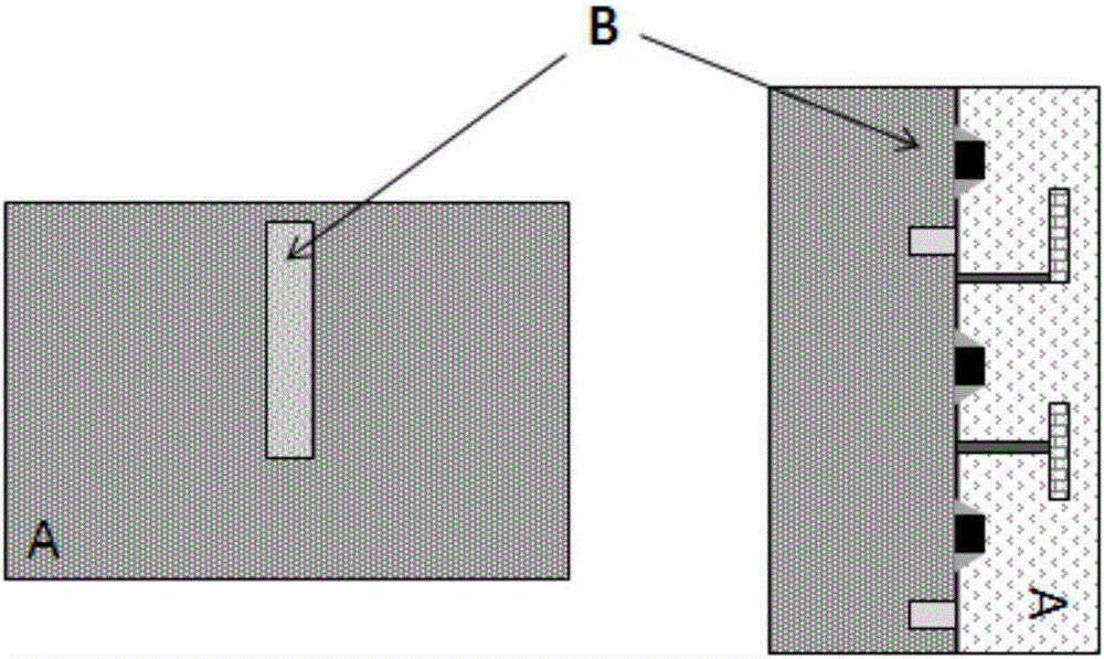
[0045] First, if Figure 2a As shown, observe the plane of the sample O in the FIB and look for the target region T. The section of the sample O is prepared by means of slices or masks, so that the section is constantly approaching the target T, and the final section is 1-10 microns away from the target. The target area includes the active region dislocation D1 and the gate oxide layer defect D2 that need to be observed in this analysis.

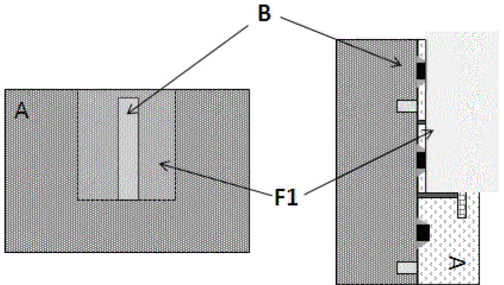
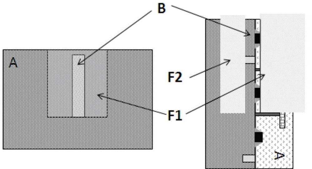
[0046] Next, rotate the sample and continue cutting on the plane of the sample by the ion beam of the FIB. At this time, a cutting plane parallel to the silicon substrate interface begins to form, starting from the top layer of the sample until the Poly layer is completely exposed, as shown in Fig. Figure...


PUM


Abstract

The invention provides a preparation method of a planar TEM sample. The method comprises the steps of: preparing a sample, enabling the cross section of a fracture surface of the sample to be close to a target area, cutting the sample to expose a Poly layer, carrying out wet method corrosion, removing Poly, preparing a first cutting surface, cutting the sample, preparing a second cutting surface in a substrate, and finally completing the planar TEM sample. The new method based on the prior art is provided by the invention for TEM analysis which is carried out for observing gate oxide defects and silicon substrate dislocation below polycrystalline Poly, the influences of Poly crystal lattices to TEM observation are removed by means of Poly corrosion, and the detects in the gate oxide can be accurately positioned by the corrosion of a corrosive agent to the substrate. By adopting the method, the quality and the success rate of failure analysis in the type are improved.

Description

technical field [0001] The invention relates to a preparation method of a transmission electron microscope (TEM) plane sample in integrated circuit failure analysis (FA). Background technique [0002] Today, with the continuous development of integrated circuit IC manufacturing processes, due to the continuous reduction in device size, it is becoming more and more difficult to analyze the cause of its failure, because physical failure analysis (PFA) is often difficult to find obvious failure characteristics or failure points. At this time, it is necessary to use a variety of failure analysis tools comprehensively, such as optical emission microscope (EMMI), light-induced resistance change (OBRICH), transmission electron microscope (TEM), scanning electron microscope (SEM), focused ion beam microscope (FIB), Energy Spectrometer (EDS), etc. Find the real failure cause of the device through a combination of multiple tools. Among many PFA tools, TEM has sub-nanometer high-reso...

Claims


Application Information

Patent Timeline
Patent Type & Authority Applications(China)
IPC IPC(8): G01Q30/20
Inventor 陈强陈胜
Owner SHANGHAI HUALI MICROELECTRONICS CORP
Why Eureka
Try Eureka