Jumper-free circuit for program running and JTAG program downloading
A technology of program download and program operation, applied in the direction of program loading/starting, program control device, and the generation of response errors, etc., can solve the problems affecting the normal operation of the watchdog circuit, the virtual connection of the contact circuit, and the increase of time-consuming, etc. Achieve the effect of saving download and debugging time, jumper-free, and low cost
- Summary
- Abstract
- Description
- Claims
- Application Information
AI Technical Summary
Problems solved by technology
Method used
Image
Examples
Embodiment 1
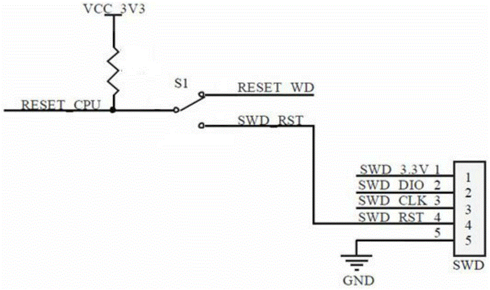
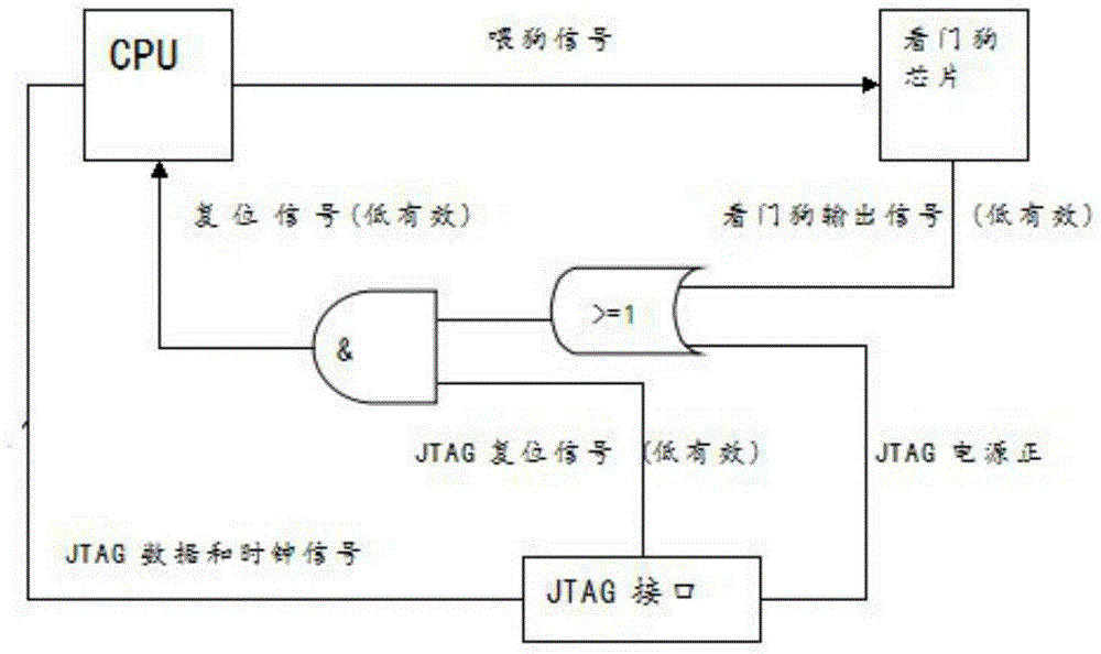
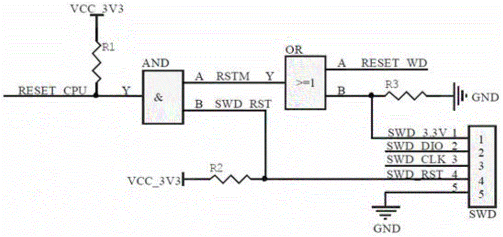
[0029] The jumper-free circuit for program running and JTAG program download includes CPU, watchdog chip, and JTAG programmer. The CPU outputs a feed signal to the watchdog chip, and the power signal SWD_3.3V of the JTAG programmer is pulled down by the third Resistor R3 is grounded and connected with the watchdog reset signal RESET_WD output by the watchdog chip to output the first signal RSTM after the OR gate, and the first signal RSTM is the same as the JTAG reset signal SWD_RST output by the JTAG writer through the AND gate. The second signal RESET_CPU is input to the CPU as a CPU reset signal. In addition, the JTAG reset signal SWD_RST is connected to the system power supply VCC_3.3V through the second pull-up resistor R2, and the second signal RESET_CPU is connected to the system power supply VCC_3.3V through the first pull-up resistor R1.
Embodiment 2
[0031] The jumper-free circuit for program running and JTAG program download includes CPU, watchdog chip, and JTAG programmer. The CPU outputs the feed signal to the watchdog chip, and the power signal SWD_3.3V of the JTAG programmer is connected to diode D2 The anode of the watchdog chip, the watchdog reset signal RESET_WD output by the watchdog chip is connected to the cathode of the diode D2 through the sixth resistor R6; the cathode of the diode D2 is connected to the first cathode input of the common anode Schottky diode D1, JTAG programming The JTAG reset signal SWD_RST output by the device is connected to the second cathode input terminal of the common anode Schottky diode D1, the JTAG reset signal SWD_RST is connected to the system power supply VCC_3.3V through the fifth pull-up resistor R5, and the common anode Schottky diode D1 The anode is connected to the system power supply VCC_3.3V through the fourth pull-up resistor R4, and the anode of the common anode Schottky ...
PUM
 Abstract
Description
Claims
Application Information


