Printed circuit board and fabrication method thereof

A technology for printed circuit boards and manufacturing methods, applied in the directions of printed circuits, printed circuit manufacturing, printed circuit secondary processing, etc. Pad and circuit defects, stable performance, small amount of suspended nickel

Active Publication Date: 2016-01-06
GUANGZHOU FASTPRINT CIRCUIT TECH +2
View PDF6 Cites 7 Cited by
  • Summary
  • Abstract
  • Description
  • Claims
  • Application Information

AI Technical Summary

Problems solved by technology

However, the nickel-gold layer is an anti-corrosion layer in the etching process. After the outer layer of the conventional hydraulic gold process is etched, there will be side erosion and over-etching. When the nickel-gold layer collapses or falls off during subsequent use or transportation, there will be risks of defects in the appearance of pads/lines and short circuits during t

Method used


Image

  • Printed circuit board and fabrication method thereof
  • Printed circuit board and fabrication method thereof
  • Printed circuit board and fabrication method thereof

Examples


Embodiment Construction

[0033] Embodiments of the present invention are described in detail below:

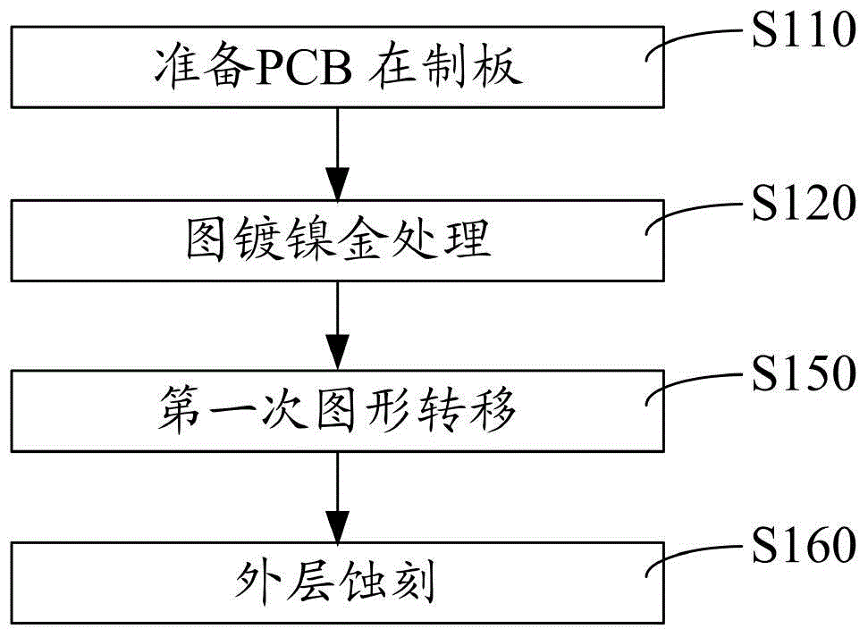
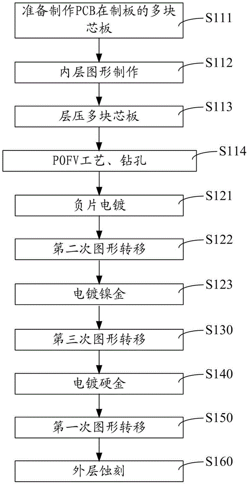
[0034] Such as figure 1 , figure 2 Shown, a kind of manufacturing method of printed wiring board comprises the following steps:

[0035] S110 Prepare PCB in process;

[0036] Specifically, the steps of preparing the PCB-in-process include:

[0037] S111 Prepare to make multiple core boards of the PCB in process;

[0038] S112 Inner layer graphic production: inner layer graphic production through inner layer graphic transfer, inner layer etching and other processes;

[0039] S113 Lamination of multiple core boards: stacking multiple core boards, moving the laminated multiple core boards into a pressing furnace for pressing by hot pressing to form a multi-layer board;

[0040] S114POFV process and drilling: make holes according to the design requirements;

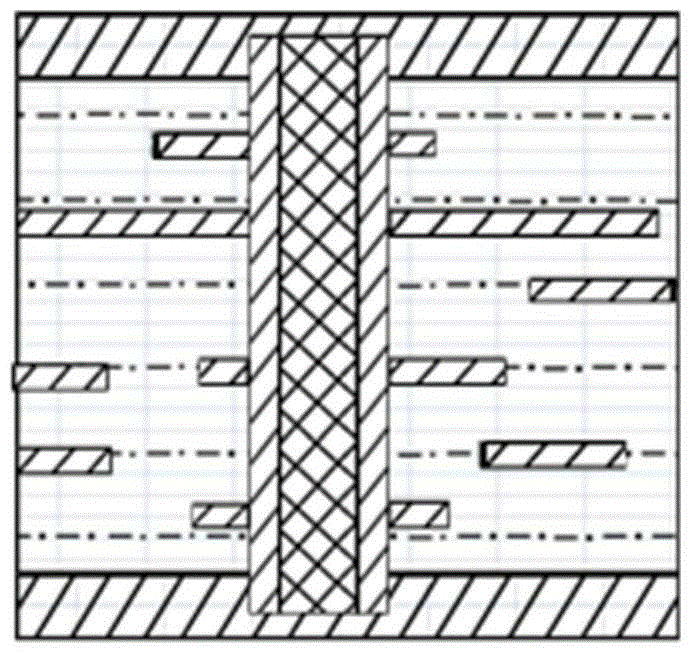
[0041] Adopt the above-mentioned process to prepare the PCB in-process board, and prepare the cross-sectional schematic diagram of the circui...


PUM


Abstract

The invention discloses a printed circuit board and a fabrication method thereof. The fabrication method of the printed circuit board includes following steps: preparing a PCB making plate; performing coating nickel-gold processing: electroplating a nickel layer and a gold layer in sequence in an area in need of electroplating nickel-gold patterns on the making plate of the PCB, and forming a nickel-gold cover head; performing the first pattern transfer: mounting a first external layer dry film on the making plate of the PCB after coating nickel-gold processing, and the outer edge width of the pattern area of the first external layer dry film being wider than the outer edge width of the nickel-gold cover head; and external layer etching: obtaining a whole line pattern via etching. The fabrication method of the printed circuit board is applicable to the whole line pattern, the suspension of nickel of a pad and the line can be prevented, or the nickel-suspension amount is small, and the problem of pad and line loss is improved. According to the printed circuit board, the suspension of nickel of the pad and the line can be prevented, or the nickel-suspension amount is small, pad and line loss is avoided, and the performance is stable and safe during usage.

Description

technical field [0001] The invention relates to the field of printed circuit boards, in particular to a printed circuit board and a manufacturing method thereof. Background technique [0002] A printed circuit board (Printed Circuit Board, PCB), also known as a printed circuit board, is a provider of electrical connections for electronic components. In the process of PCB production, it is generally necessary to apply graphic electroplating (picture plating) copper nickel gold + electroplating hard gold process (referred to as hydraulic gold process). However, the nickel-gold layer is an anti-corrosion layer in etching. After the outer layer of the conventional hydraulic gold process is etched, there will be side erosion and over-etch phenomenon. When the nickel-gold layer collapses or falls off during subsequent use or transportation, there will be risks of defects in the appearance of pads / lines and short circuits during testing. Traditionally, the problem of overhanging ...

Claims


Application Information

Patent Timeline
IPC IPC(8): H05K3/06H05K3/24
CPCH05K3/06H05K3/24H05K3/241H05K2203/1461
Inventor 李娟李艳国陈蓓
Owner GUANGZHOU FASTPRINT CIRCUIT TECH
Why Eureka
Try Eureka