

Liquid crystal display apparatus and method of manufacturing the same via short-circuited bus lines
a technology of liquid crystal display and bus line, which is applied in the direction of chemistry apparatus and processes, identification means, instruments, etc., can solve the problems of not having not having a member sharing of tft substrate or the like, and not having an idea of using a common tft substrate in the conventional art. , to achieve the effect of enhancing the production efficiency and yield of such panels
- Summary
- Abstract
- Description
- Claims
- Application Information
AI Technical Summary
Benefits of technology
Problems solved by technology
Method used
Image

Examples
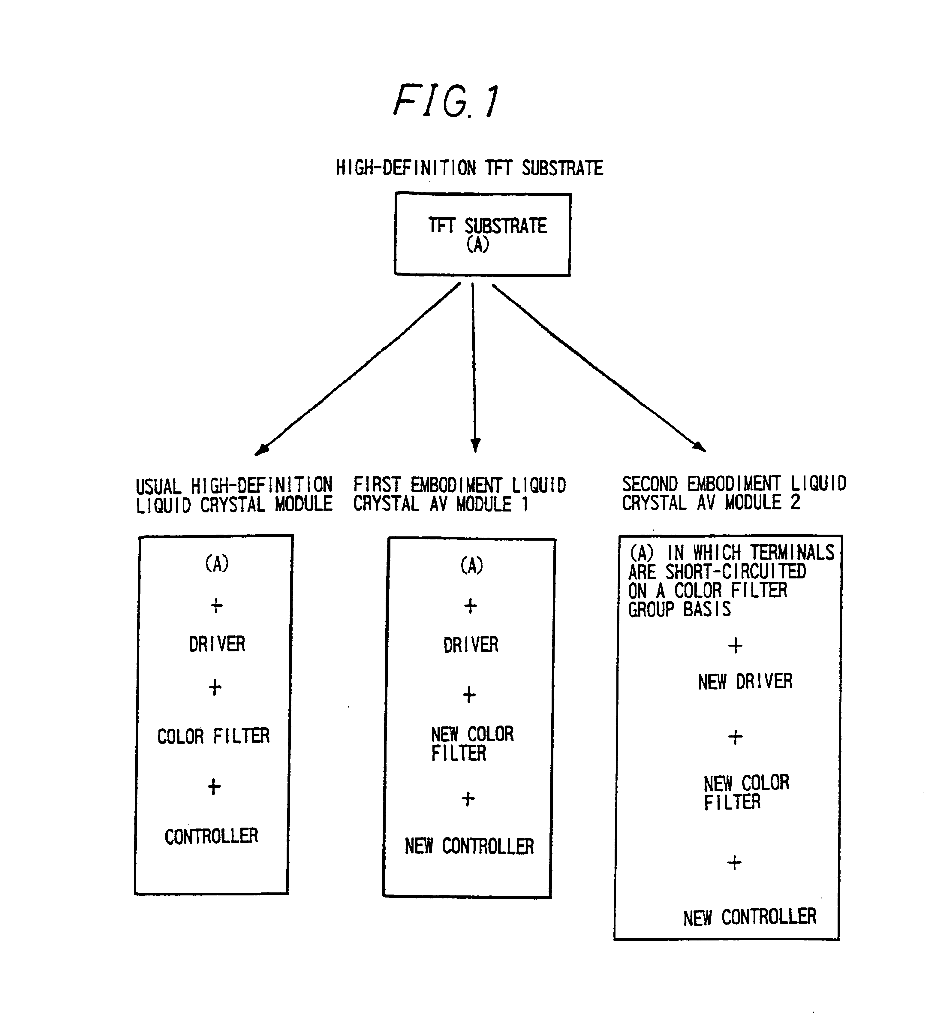
first embodiment
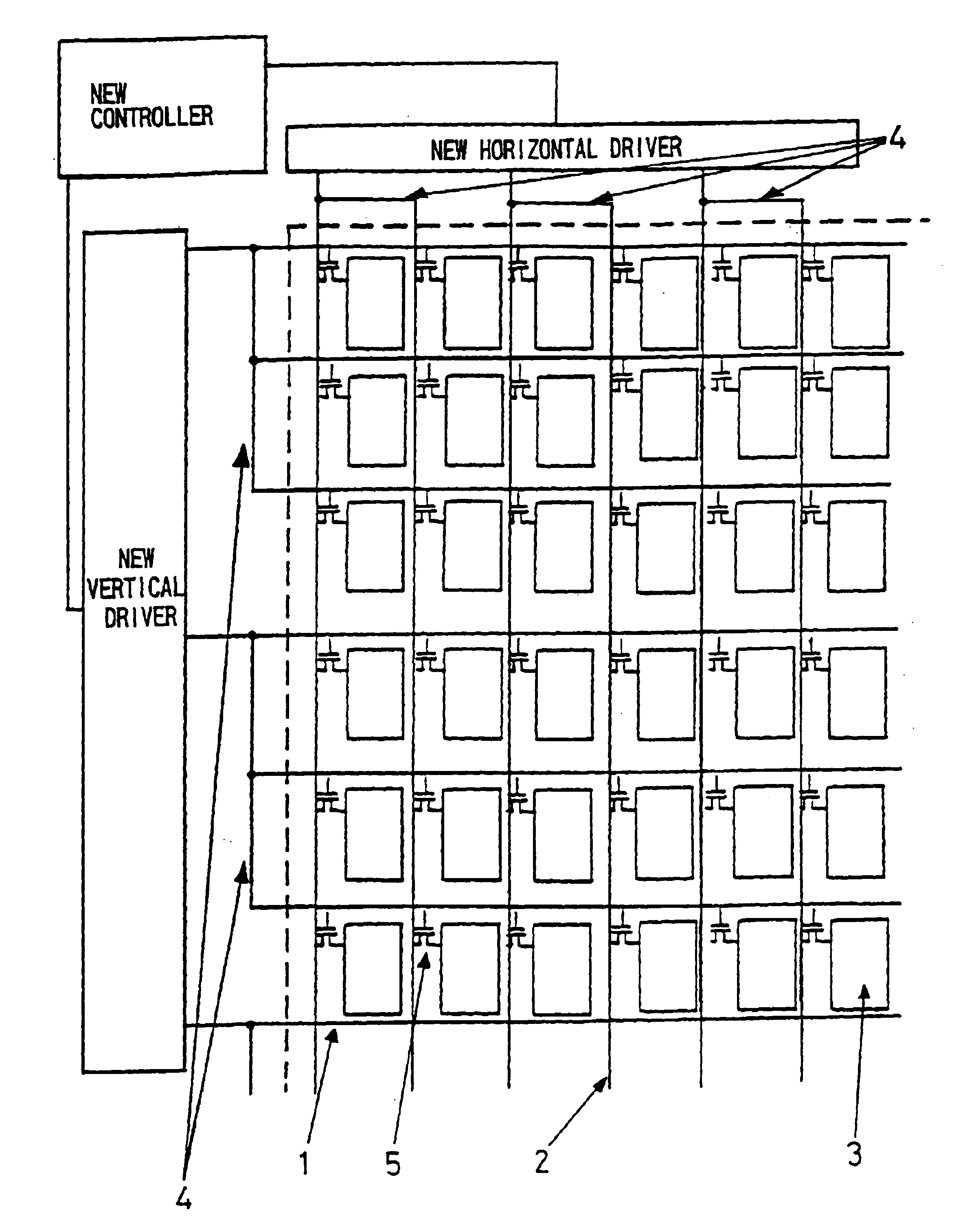
In the first embodiment, a liquid crystal AV module is manufactured by changing only the color filters and controller from among the components used in the high-definition liquid crystal module into corresponding ones adapted for an AV module.
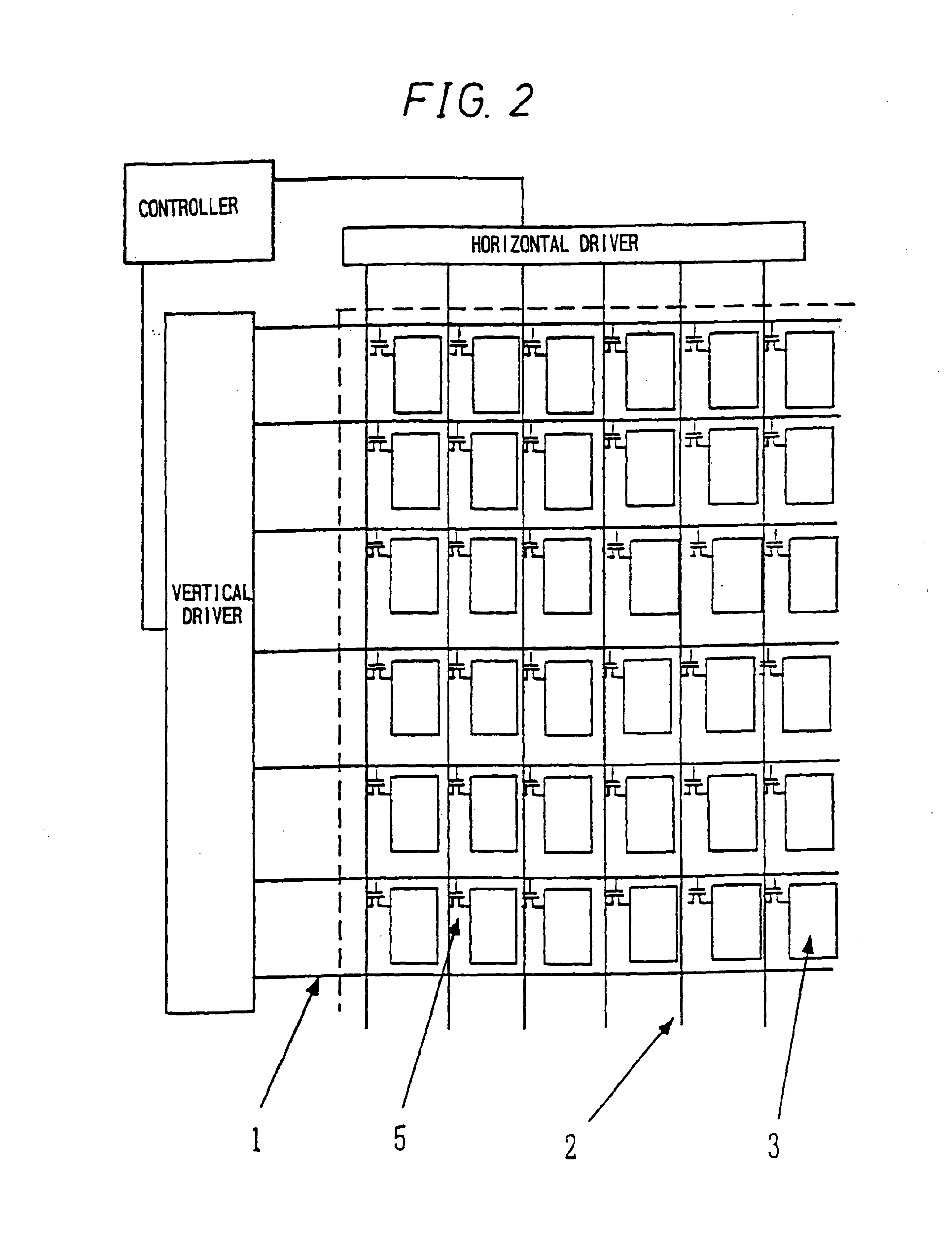
As shown in FIG. 5, the high-definition TFT substrate (A) is laminated as a counter substrate with new color filters wherein colors for R, G and B are allocated to a corresponding group of pixels and that one pixel group consists of a plurality of pixels. For convenience of illustration of the arrangement of color filters, FIG. 5 shows gate bus lines 1, source bus lines 2, pixels 3 and TFT devices 5, which are all absent on the counter substrate. Each of the pixels 3 is what is called a pixel electrode.
In this embodiment, an example is shown wherein one pixel group consists of pixels of 3 rows×6 columns. However, the invention is not limited to this value.
In turn, as shown in FIG. 4, horizontal and vertical drivers used for the high-definition ...
second embodiment
In the second embodiment, a liquid crystal AV module is manufactured by changing the color filters, drivers and controller of the components used in the high-definition liquid crystal module into corresponding ones adapted for an AV module and by short-circuiting terminals of the high-definition TFT substrate on a group basis.
The high-definition TFT substrate (A) is modified by short-circuiting the terminals of the source bus lines and gate bus lines on a group basis using a photo step. Specifically, in the formation of pixel electrodes, a photomask used to form the pixel groups of a conventional high-definition panel is substituted with a photomask wherein terminals are short-circuited on a group basis. Thus, a TFT substrate adapted for the purpose can be obtained only by changing one photomask.
The TFT substrate thus obtained is shown in FIG. 6. As shown in FIG. 7, the TFT substrate is laminated with a new color filters wherein R, G and B colors are allocated to corresponding pixel...
PUM
| Property | Measurement | Unit |
|---|---|---|
| color | aaaaa | aaaaa |
| polarity | aaaaa | aaaaa |
| sizes | aaaaa | aaaaa |
Abstract
Description
Claims
Application Information