Wavelength conversion device, manufacture method thereof, correlative light-emitting device, and projection system

A technology of a wavelength conversion device and a light-emitting layer is applied in the fields of wavelength conversion devices and their preparation, related light-emitting devices, and projection devices. The effect of interface thermal resistance

Active Publication Date: 2016-01-27
APPOTRONICS CORP LTD
View PDF6 Cites 49 Cited by
  • Summary
  • Abstract
  • Description
  • Claims
  • Application Information

AI Technical Summary

Problems solved by technology

[0005] However, it has been found in practical applications that this wavelength conversion device, which uses inorganic scattering materials as the reflective layer and glass materials as the bonding agent between phosphor powder and inorganic scattering materials, can remain stable under high-power laser irradiation, but its Poor heat dissipation and low luminous efficiency

Method used


Image

  • Wavelength conversion device, manufacture method thereof, correlative light-emitting device, and projection system
  • Wavelength conversion device, manufacture method thereof, correlative light-emitting device, and projection system
  • Wavelength conversion device, manufacture method thereof, correlative light-emitting device, and projection system

Examples


Embodiment 1

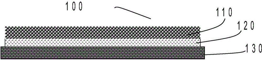
[0039] See figure 1 , figure 1 It is a schematic structural diagram of Embodiment 1 of the wavelength conversion device of the present invention. As shown in the figure, the wavelength conversion device 100 includes a light emitting layer 110 , a diffuse reflection layer 120 and a ceramic substrate 130 . Wherein the light emitting layer 110 is a sintered body comprising phosphor powder and the first glass powder, and the diffuse reflection layer 120 is a sintered body comprising white scattering particles and the first glass powder.

[0040] After the excitation light emitted by the excitation light source is incident on the light-emitting layer 110, the phosphor powder is excited to emit the subject light. After the excited light and the unexcited excitation light pass through the light-emitting layer 110, they are incident on the diffuse reflection layer 120, and then are reflected back to the light-emitting layer 110, wherein the excited light and part of the unexcited ex...

Embodiment 2

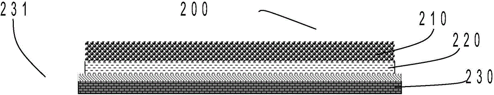
[0075] See figure 2 , figure 2 It is a schematic structural diagram of Embodiment 2 of the wavelength conversion device of the present invention. As shown in the figure, the wavelength conversion device 200 includes a light-emitting layer 210 , a diffuse reflection layer 220 and a ceramic substrate 230 . Different from Embodiment 1, in this embodiment, the wavelength conversion device 200 also includes an interface bonding layer 231 .

[0076] In this embodiment, the ceramic substrate 230 is an aluminum nitride substrate, the interface bonding layer 231 is an alumina layer, and the alumina layer 231 is formed on the surface of the aluminum nitride substrate 230 and is a part of the ceramic substrate 230 .

[0077] The preparation method of the wavelength conversion device 200 in this embodiment is as follows:

[0078] Step 1: providing an aluminum nitride substrate 230, and performing surface densification treatment on the aluminum nitride substrate 230, specifically inclu...

Embodiment 3

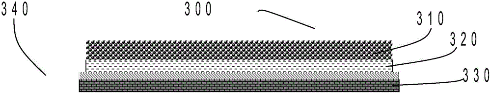
[0086] See image 3 , image 3 It is a structural schematic diagram of Embodiment 3 of the wavelength conversion device of the present invention. As shown in the figure, the wavelength conversion device 300 includes a light emitting layer 310 , a diffuse reflection layer 320 , a ceramic substrate 330 and an interface bonding layer 340 . Different from the second embodiment, in this embodiment, the interface bonding layer 340 is a layer structure independent of the ceramic substrate 330 .

[0087] In this embodiment, the interface bonding layer 340 is a glass bonding layer, and the glass bonding layer includes the same first glass frit as that in the diffuse reflection layer 320 .

[0088] Due to the problem of the preparation process, when the diffuse reflection layer 320 is fired on the ceramic substrate 330 , there may be white scattering particles in direct contact with the ceramic substrate 330 . Since the white scattering particles do not undergo a softening and reshap...


PUM

PropertyMeasurementUnit
thicknessaaaaaaaaaa
reflectanceaaaaaaaaaa

Abstract

The invention discloses a wavelength conversion device, a manufacture method thereof, a correlative light-emitting device, and a projection system. The wavelength conversion device comprises a light-emitting layer, a diffuse reflection layer, and a ceramic substrate which are successively stacked. The light-emitting layer comprises fluorescent powder and first glass powder. The volume fraction of the fluorescent powder to the light-emitting layer is from 14.1 to 38.7 percent. The diffuse reflection layer comprises white scattering particles and the first glass powder. The volume fraction of the white scattering particles to the diffuse reflection layer is from 22.0 to 62.9 percent. The coefficient of linear expansion of the ceramic substrate is greater than that of the first glass powder but less than those of the ceramic substrate and the white scattering particles. By adjustment of the volume fraction of the fluorescent powder in the light-emitting layer and the volume fraction of the white scattering particles in the diffuse reflection layer, the light-emitting layer and the diffuse reflection layer have high enough light-emitting efficiency and reflectivity and low internal thermal resistance and interface thermal resistance so as to achieve a beneficial effect of obtaining emergent light with high light-emitting efficiency.

Description

technical field [0001] The invention relates to the field of display and illumination, in particular to a wavelength conversion device and a preparation method thereof, a related light-emitting device and a projection device. Background technique [0002] With the development of display and lighting technology, the original LED or halogen bulb as a light source is increasingly unable to meet the high power and high brightness requirements of display and lighting. Visible light of various colors can be obtained by using excitation light emitted by a solid-state light source such as LD (Laser Diode, laser diode) to excite wavelength conversion materials, and this technology is increasingly used in lighting and display. This technology has the advantages of high efficiency, low energy consumption, low cost, and long life, and is an ideal alternative to existing white or monochromatic light sources. [0003] In the prior art, the light source of laser excitation wavelength conv...

Claims


Application Information

Patent Timeline
Patent Type & Authority Applications(China)
IPC IPC(8): G03B21/20F21V9/08G02B5/02
CPCC03C14/006G02B5/0242G02B5/0284G02B5/0294
Inventor 田梓峰李乾许颜正
Owner APPOTRONICS CORP LTD
Why Eureka
Try Eureka