Laser pattern device and laser pattern optical mesh of invisible sensor layer of touch panel

A touch panel and sensing layer technology, applied in the field of laser patterning, can solve problems such as damage or pollution, substrate bending, etc., and achieve the effects of simplifying the process, transferring patterns accurately, and saving production costs

Active Publication Date: 2016-01-27
HANNSTAR DISPLAY NANJING +1
View PDF5 Cites 2 Cited by
  • Summary
  • Abstract
  • Description
  • Claims
  • Application Information

AI Technical Summary

Problems solved by technology

[0004] The purpose of the present invention is to provide a laser patterning device and a laser patterning grid for the invisible sensing layer of a touch panel, which can simplify the process and save production costs, and can obtain more accurate transfer patterns, while avoiding It is known that sending the substrate to the oven for tempering can easily cause problems such as bending, damage or contamination of the substrate

Method used


Image

  • Laser pattern device and laser pattern optical mesh of invisible sensor layer of touch panel
  • Laser pattern device and laser pattern optical mesh of invisible sensor layer of touch panel
  • Laser pattern device and laser pattern optical mesh of invisible sensor layer of touch panel

Examples


Embodiment Construction

[0038] The laser patterning equipment and the laser patterning grid of the invisible sensing layer of the touch panel according to the preferred embodiment of the present invention will be described below with reference to the relevant drawings, wherein the same elements will be described with the same reference symbols .

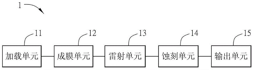
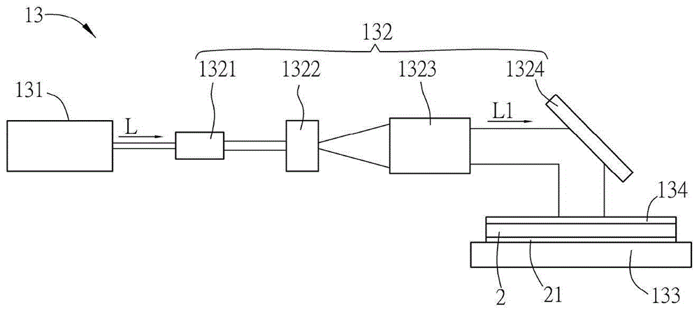
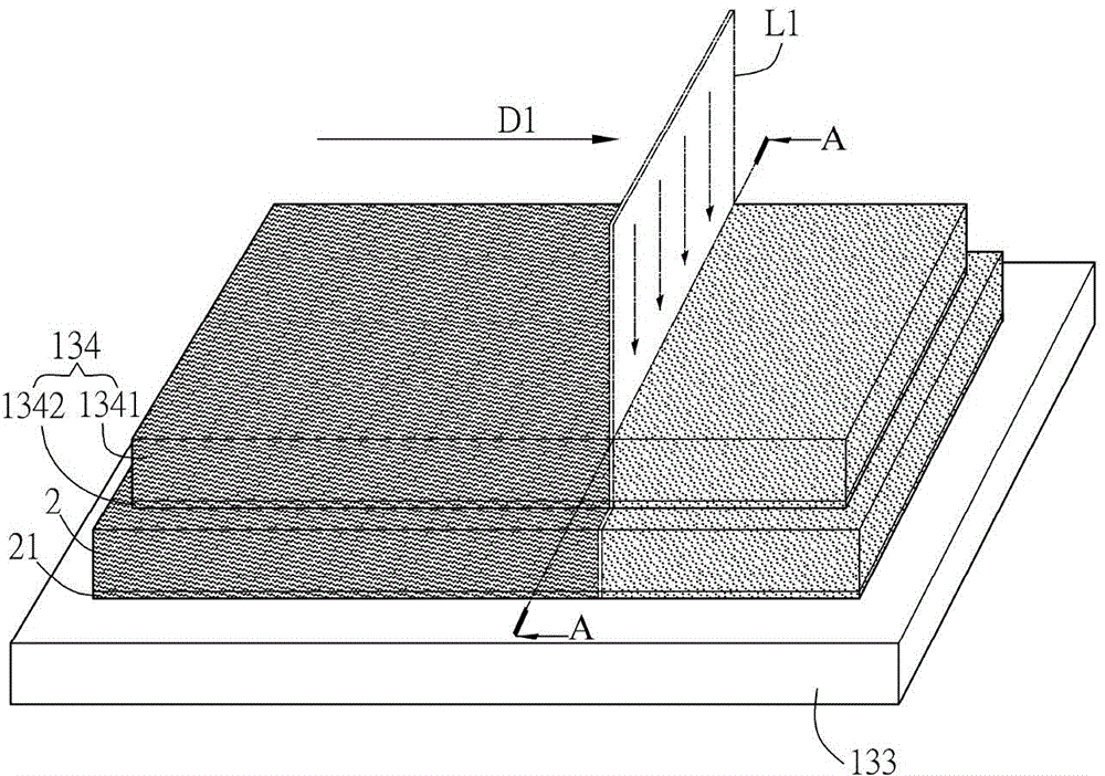
[0039] figure 1 It is a functional block diagram of the laser patterning device for the invisible sensing layer of the touch panel according to the preferred embodiment of the present invention. Please refer to figure 1 As shown, the laser patterning device 1 can be used to form pixel electrodes of a display panel, touch electrodes (touch sensing structure) of a touch panel, or other conductive structures such as wires or ground wires. In this embodiment, it is described by taking the formation of an invisible sensor layer of a touch panel as an example. Here, the laser patterning device 1 includes a loading unit 11 , a film forming unit 12 , a laser uni...


PUM

PropertyMeasurementUnit
diameteraaaaaaaaaa
lengthaaaaaaaaaa

Abstract

The names of the invention are a laser pattern device and a laser pattern optical mesh of an invisible sensor layer of a touch panel. The laser pattern device of the invisible sensor layer of the touch panel comprises a loading unit, a deposition unit, a laser unit and an etching unit; the loading unit is provided with a substrate; a sensor layer is formed by the deposition unit on the substrate; the laser unit performs the laser annealing treatment on a bent anti-interference patch pattern and a sensor layer predetermined pattern of the sensor layer to form a structure changing layer; and the etching unit removes the part of sensor layer except the anti-interference patch pattern and the sensor layer predetermined pattern to form the invisible sensor layer of the touch panel. The laser pattern device provided by the invention can obtain relatively accurate transfer patterns, and can avoid the problems of the common situation that the substrate is likely to be bent, damaged or polluted caused by the fact that the substrate is sent to an oven to be annealed.

Description

【Technical field】 [0001] The invention relates to a laser patterning technology, in particular to a laser patterning device and a laser patterning grid of an invisible sensing layer of a touch panel. 【Background technique】 [0002] In recent years, touch technology has gradually been widely used in general consumer electronics products, such as mobile communication devices, digital cameras, digital music players (MP3), personal digital assistants (PDA), satellite navigation devices (GPS), Hand-held PCs (hand-held PCs), tablet PCs (tablets), and even brand-new super mobile computers (UltraMobilePC, UMPC), etc. Touch technology can be applied to the display panel in various forms, such as adding a touch panel on the display panel (plug-in type), or making a touch sensing unit directly on the display panel (embedded type, also divided into on -cell and in-cell). [0003] However, the process of making the touch sensing unit needs to be formed through film formation, exposure,...

Claims


Application Information

Patent Timeline
Patent Type & Authority Applications(China)
IPC IPC(8): G06F3/041G02F1/1333H01L21/67
Inventor 卢添荣
Owner HANNSTAR DISPLAY NANJING
Why Eureka
Try Eureka