

Method for forming semiconductor structure
A technology of semiconductor and dummy gate structure, applied in semiconductor/solid-state device manufacturing, electrical components, circuits, etc., can solve problems such as poor reliability and unstable performance of fin field effect transistors
- Summary
- Abstract
- Description
- Claims
- Application Information
AI Technical Summary
Problems solved by technology
Method used
Image

Examples
Embodiment Construction
[0031] As mentioned in the background, the FinFETs formed in the prior art have unstable performance and poor reliability.
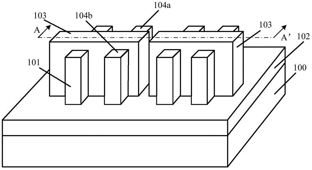
[0032] In order to further reduce the size of the semiconductor device and increase the integration of the semiconductor device, a high-K metal gate (High-K Metal Gate, HKMG for short) structure is introduced into the transistor. Please continue to refer figure 1 , the gate structure 103 includes: a gate dielectric layer located on the sidewall and top surface of the fin 101 , and a gate layer located on the surface of the gate dielectric layer. When the gate structure 103 is a high-K metal gate structure, the material of the gate dielectric layer is a high-K dielectric material, and the material of the gate layer is metal.
[0033]The high-K metal gate structure needs to be formed by a gate last (GateLast) process, that is, a dummy gate structure straddling the fin 101 is first formed on the sidewall and top surface of the fin 101, and then the dummy g...
PUM
 Abstract
Description
Claims
Application Information