Mixed wafer level vacuum packaging method and structure
A vacuum packaging, wafer-level technology, applied in the manufacture of electrical components, electrical solid devices, semiconductor/solid devices, etc., can solve the problems of wasting infrared filters, low efficiency, poor performance, etc., to reduce packaging volume and reduce packaging Cost, the effect of improving packaging efficiency
- Summary
- Abstract
- Description
- Claims
- Application Information
AI Technical Summary
Problems solved by technology
Method used
Image

Examples
Embodiment 1
[0067] This embodiment provides a hybrid wafer-level vacuum packaging method, including the following steps:
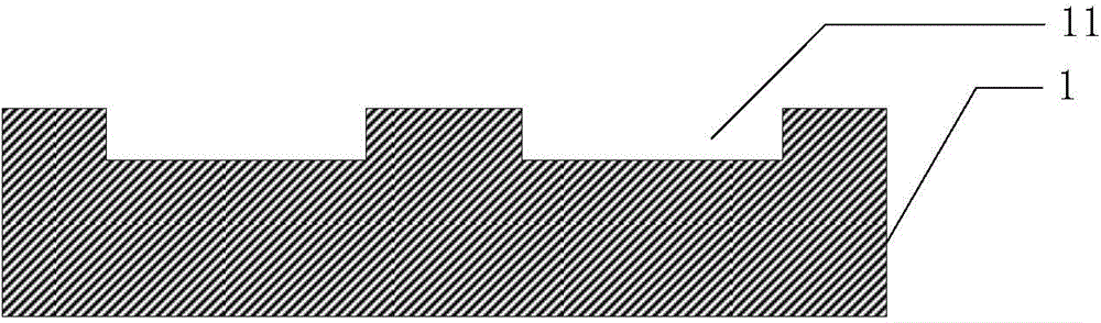
[0068] First perform step a), provide a substrate sheet, and form a chip package cavity in the substrate sheet;
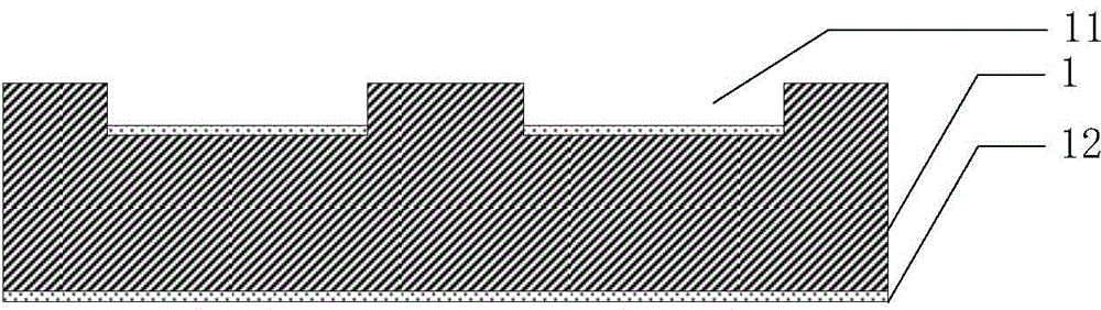
[0069] Then proceed to step b), making a getter film in the chip package cavity of the substrate sheet;
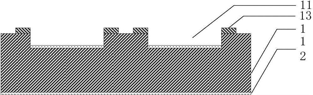
[0070] Then proceed to step c), providing a chip to be packaged that has passed the test including the substrate and the device area; wherein, if necessary, metal pillars for electrical leads need to be formed in the substrate of the chip to be packaged;
[0071] Finally, step d) is carried out, providing a vacuum device, after aligning the chip to be packaged and the chip packaging cavity, vacuumize, activate the getter, heat and pressurize, and bond the substrate and the chip through the bonding structure Describe the chip to be packaged.
[0072] As an example, in another embodiment, step a) may also include the step of forming a limiting groove i...
Embodiment 2
[0105] like Figure 2a ~ Figure 2g As shown, this embodiment provides a hybrid wafer-level vacuum packaging method, the basic steps of which are as in Embodiment 1, wherein the main difference between the packaging method of this embodiment and Embodiment 1 is that in step 1) of Embodiment 1 In addition to making the chip package cavity 11, a vacuum buffer cavity 15 is also made around the chip package cavity 11 to prolong the service life of the device.
[0106] Specifically, this embodiment includes the following steps:
[0107] like Figure 2a As shown, step 1) is first carried out, and on the infrared filter 1 (double-thrown silicon wafer or germanium wafer or zinc sulfide wafer), use corrosion, etching or laser processing methods to make a chip package on the surface of the infrared filter 1 Chamber 11 and vacuum buffer chamber 15; in the subsequent process (in the final vacuum packaging step), an appropriate amount of getter can be placed and fixed in the cavity of the...
Embodiment 3
[0116] like Figure 3a ~ Figure 3g As shown, this embodiment provides a hybrid wafer-level vacuum packaging method, the basic steps of which are as in Embodiment 1, wherein the main difference between the packaging method of this embodiment and Embodiment 1 is that in step 1) of Embodiment 1 In addition to making the chip package cavity 11 in the infrared filter 1, a limit groove 16 for limiting the position of the chip is also made.
[0117] Specifically, this embodiment includes the following steps:
[0118] like Figure 3a As shown, step 1) is first carried out, and on the infrared filter 1 (double-thrown silicon wafer or germanium wafer or zinc sulfide wafer), use corrosion, etching or laser processing methods to make a chip package on the surface of the infrared filter 1 Cavity 11 and limiting groove 16;
[0119] like Figure 3b As shown, then carry out step 2), make infrared anti-reflection film 12 at the bottom of chip package cavity 11 and the lower surface of infr...
PUM
 Abstract
Description
Claims
Application Information
 - Generate Ideas
- Intellectual Property
- Life Sciences
- Materials
- Tech Scout
- Unparalleled Data Quality
- Higher Quality Content
- 60% Fewer Hallucinations
Browse by: Latest US Patents, China's latest patents, Technical Efficacy Thesaurus, Application Domain, Technology Topic, Popular Technical Reports.
© 2025 PatSnap. All rights reserved.Legal|Privacy policy|Modern Slavery Act Transparency Statement|Sitemap|About US| Contact US: help@patsnap.com