Manufacturing method for quantum dot display panel

一种显示面板、制作方法的技术,应用在对表面涂布液体的装置、静态指示器、仪器等方向,能够解决喷墨打印设备要求很高、量子点层图形化、不能大规模生产等问题,达到原料制备及制作工艺简单、提升色饱和度与色域、节约成本与制程时间的效果

Active Publication Date: 2016-02-10
TCL CHINA STAR OPTOELECTRONICS TECH CO LTD
View PDF6 Cites 20 Cited by
  • Summary
  • Abstract
  • Description
  • Claims
  • Application Information

AI Technical Summary

Problems solved by technology

For example, the patent CN102944943A and the patent US20150002788A1 both proposed a technical solution to replace the color filter film (ColorFilter) with a patterned quantum dot layer to achieve the purpose of color display, but these patents did not carry out the method of patterning the quantum dot layer. illustrate
[0004] Patent CN103226260A provides a method of dispersing quantum dots in photoresist and patterning the quantum dot layer by photolithography, but quantum dots are dispersed in photoresist, because there is an initiator (initiation) in the photoresist , polymer monomer (monomer), polymer (polymer), additive (additive) and other polymer materials, the surface chemical environment of quantum dots is complex, which greatly affects the luminous efficiency of quantum dots
In addition to the above methods, quantum dot graphics can also be produced by transfer printing, screen printing, etc., but the resolution of the quantum dot graphics obtained by the transfer printing method is not high, the edges of the graphics are jagged, and the quantum dot layer and the matrix Adhesion needs to be improved; while the method of inkjet printing to form a patterned quantum dot layer has high requirements on inkjet printing equipment, how to ensure the stability of inkjet ink droplets and printing accuracy still has technical barriers, and it still cannot be mass-produced

Method used


Image

  • Manufacturing method for quantum dot display panel
  • Manufacturing method for quantum dot display panel
  • Manufacturing method for quantum dot display panel

Examples


Embodiment Construction

[0038]In order to further illustrate the technical means adopted by the present invention and its effects, the following describes in detail in conjunction with preferred embodiments of the present invention and accompanying drawings.

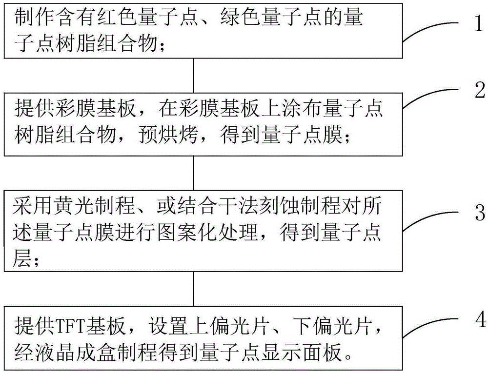
[0039] see figure 1 , the invention provides a method for manufacturing a quantum dot display panel, comprising the steps of:

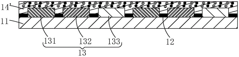
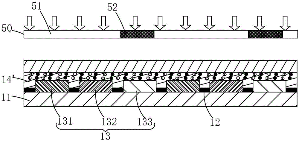
[0040] Step 1, uniformly mixing the surface-modified red quantum dots, surface-modified green quantum dots, alkali-soluble resin, solvent, dispersant, and additives in a certain proportion to obtain a quantum dot resin composition;

[0041] Specifically, the red quantum dots and green quantum dots in the quantum dot resin composition are II-VI semiconductor materials (such as CdS, CdSe, HgTe, ZnS, ZnSe, ZnTe, HgS), III-V semiconductor materials ( Such as one or more of InP, InAs, GaP, GaAs), IV-VI nano-semiconductor materials, the particle size of the red quantum dots and green quantum dots is 1-10nm.

[0042] Specif...


PUM

PropertyMeasurementUnit
particle diameteraaaaaaaaaa

Abstract

The invention provides a manufacturing method for a quantum dot display panel. By means of the existing yellow light manufacturing procedure of a color light filter or in combination with the dry method etching manufacturing procedure, a resin composition containing red and green quantum dots for surface finish is manufactured to obtain a quantum dot layer with an exquisite graph structure. Compared with other existing manufacturing method for the quantum dot display panel, the manufacturing method has the advantages that the raw material preparing and manufacturing process is simple, the graph resolution is high, the display panel can be manufactured on a large scale, cost and manufacturing procedure time are saved, the quantum dots are guided into the color light filter structure, color saturation and color gamut of a display device can be effectively promoted, and the color expressive ability of the display panel is enhanced.

Description

technical field [0001] The invention relates to the field of display technology, in particular to a method for manufacturing a quantum dot display panel. Background technique [0002] With the continuous development of display technology, people have higher and higher requirements for display quality of display devices. Quantum dots (Quantum Dots, referred to as QDs) are usually spherical or quasi-spherical semiconductor nanoparticles composed of II-VI or III-V group elements, and the particle size is generally between a few nanometers and tens of nanometers. Because the particle size of QDs is smaller than or close to the exciton Bohr radius of the corresponding bulk material, a quantum confinement effect will be generated, and its energy level structure will change from the quasi-continuous structure of the bulk material to the discrete structure of the quantum dot material, resulting in QDs showing special properties of stimulated emission of light. As the size of QDs d...

Claims


Application Information

Patent Timeline
Patent Type & Authority Applications(China)
IPC IPC(8): G02F1/1335
CPCG02F1/133514G02F1/133516G02F1/133528G02F1/133531G02F1/1362G09G3/00G02F1/133617G02F2202/36G02F1/1335G02F1/133614B05D1/005G02F1/133512G02F1/133621G02F1/1339G02F1/1368G02F2202/10
Inventor 刘国和
Owner TCL CHINA STAR OPTOELECTRONICS TECH CO LTD
Why Eureka
Try Eureka