

Low-power-consumption high-PSRR band-gap reference source
A low power consumption, reference source technology, applied in the direction of adjusting electrical variables, control/regulation systems, instruments, etc., can solve the problem of low output voltage accuracy
- Summary
- Abstract
- Description
- Claims
- Application Information
AI Technical Summary
Problems solved by technology
Method used
Image

Examples
Embodiment 1
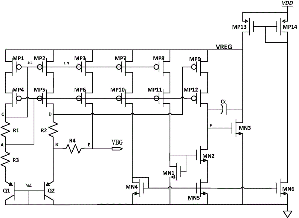
[0094] see image 3 As shown, in Embodiment 1, including the above-mentioned low power consumption high PSRR bandgap reference source circuit, its voltage feedback circuit 10 specifically includes: the seventh P-channel field effect transistor MP7, the eighth P-channel field effect transistor MP8, The ninth P-channel FET MP9, the tenth P-channel FET MP10, the eleventh P-channel FET MP11, the twelfth P-channel FET MP12, the thirteenth P-channel FET MP13, the tenth Four P-channel FETs MP14, the first N-channel FETs MN1, the second N-channel FETs MN2, the third N-channel FETs MN3, the fourth N-channel FETs MN4, and the fifth N-channel FETs The transistor MN5, the sixth N-channel field effect transistor MN6, and the compensation capacitor Cc.
[0095] Specifically, the source of the thirteenth P-channel field effect transistor MP13 is connected to the source of the fourteenth P-channel field effect transistor MP14 and connected to the external power supply VDD, and the gate of th...
Embodiment 2
[0113] Such as Figure 4 As shown, the low power consumption and high PSRR bandgap reference source circuit provided by Embodiment 2 is basically the same as the circuit shown in Embodiment 1, and the parts with the same structure will not be repeated here.
[0114] Wherein, in embodiment two, refer to Figure 4 As shown, the gate of the first N-channel field effect transistor MN1 is connected to the source of the second N-channel field effect transistor MN2. At this time, the first N-channel field effect transistor MN1 and the second N-channel field effect transistor MN2 form a Gainboost structure.
[0115] MN1 and MN2 adopt the Gainboost structure, which improves the output impedance of point F; at the same time, the Cascode current mirror composed of MP2 and MP5 also improves the output impedance of point D; the improvement of output impedance increases the loop gain and reduces C, D Gain error at two points, thereby reducing the effect of gain error on output voltage off...
PUM
 Abstract
Description
Claims
Application Information