Method of photoresist strip

A photoresist and photoresist layer technology, which is applied in the manufacture of electrical components, electrical solid-state devices, semiconductor/solid-state devices, etc., can solve the problem of long soaking time in photoresist stripping solution, increased environmental production costs, and scattered bumps. And other issues

Inactive Publication Date: 2016-02-10
CHIPBOND TECH
View PDF6 Cites 3 Cited by
  • Summary
  • Abstract
  • Description
  • Claims
  • Application Information

AI Technical Summary

Problems solved by technology

Wherein, in the process of removing the photoresist, generally the substrate covered with the photoresist layer is immersed in a photoresist stripping solution, so that the photoresist layer is swollen, cracked and peeled off from the substrate, However, according to different product requirements, the types of photoresist materials and photoresist stripping solutions used in the manufacturing process are not the same, and the conventional technology often causes the substrate to be immersed in the photoresist during the process of photoresist stripping. The resist stripping solution takes too long to cause the bumps to fall off or cause damage to the protective layer of the substrate
Conversely, if the immersion time of the substrate in the photoresist stripping solution is too short, it will easily lead to the residue of the photoresist layer, which will affect the yield of the bump manufacturing process.
In addition, in the bump manufacturing process, since the bump needs to have a certain thickness, the thickness of the photoresist layer also needs to be coated with a corresponding thickness, resulting in a longer soaking time in the photoresist stripping solution, and The amount of photoresist stripping solution used is also large, resulting in an environmental burden and an increase in production costs

Method used


Image

  • Method of photoresist strip
  • Method of photoresist strip
  • Method of photoresist strip

Examples


no. 1 example

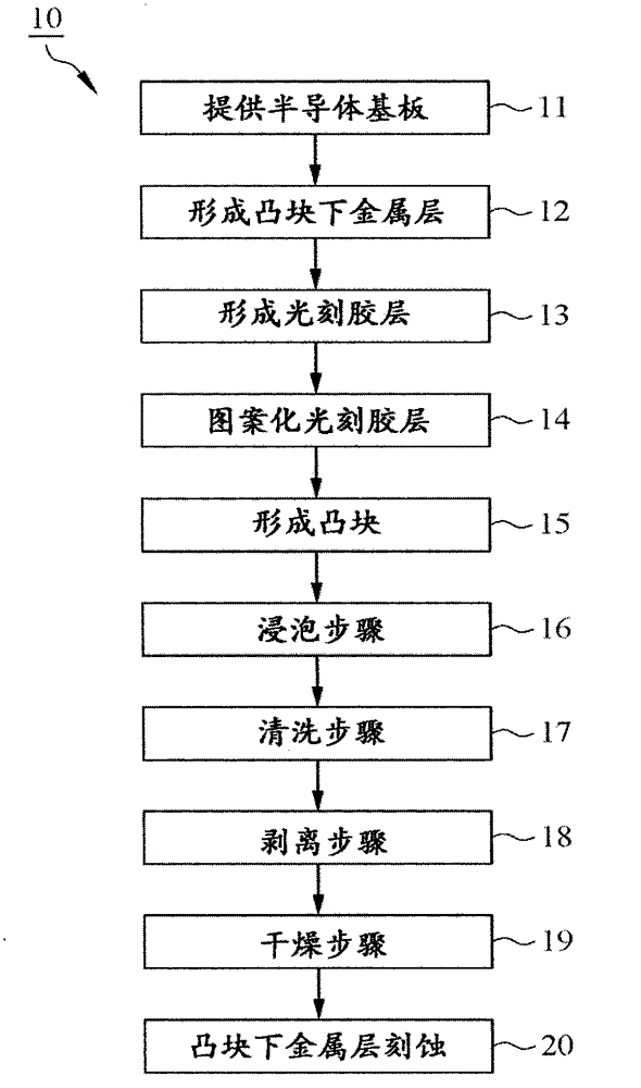
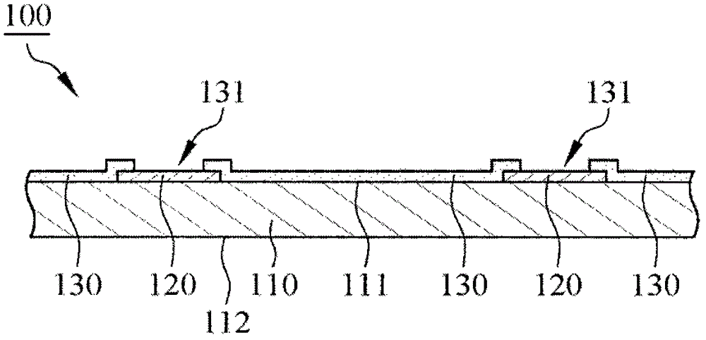
[0044] see figure 1 , is the first embodiment of the present invention, a flow chart of a photoresist stripping method 10, please refer to figure 1 and figure 2, provide a semiconductor substrate 100 in "providing a semiconductor substrate 11", wherein the semiconductor substrate 100 has a substrate 110, a bonding pad 120 and a protective layer 130, the bonding pad 120 is located on the surface 111 of the substrate 110, and the protective layer 130 covers the substrate 110 and the pad 120 , and the protective layer 130 has an opening 131 , the opening 131 exposes the pad 120 , and the pad 120 can be selected from copper, aluminum, copper alloy or other conductive materials.

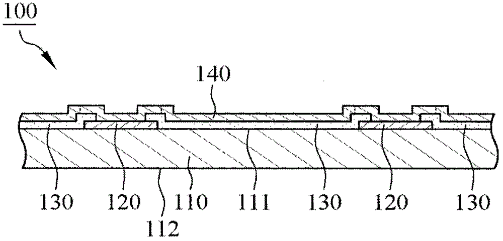
[0045] see figure 1 and image 3 In "forming the UBM layer 12", the UBM layer 140 is plated on the protective layer 130 by evaporation, sputtering, electroplating or electroless plating, and the UBM layer 140 covers the protection layer 130, and the UBM layer 140 is connected to the pad 120, wherein ...


PUM

PropertyMeasurementUnit
heightaaaaaaaaaa

Abstract

A method of photoresist strip includes providing a semiconductor substrate and performing an immerse step and a strip step, wherein the semiconductor substrate comprises a base, a bonding pad, a protective layer, an under bump metallurgy layer, a patterned photoresist layer and a bump. The patterned photoresist layer covers the under bump metallurgy layer and a lateral surface of the bump, wherein a first connection interface is formed between the patterned photoresist layer and the lateral surface of the bump, and a second connection interface is formed between the patterned photoresist layer and the under bump metallurgy layer. In the immerse step, the patterned photoresist layer contacts with a chemical solution which degrades the bond strength of the first connection interface. Therefore, in the strip step, the semiconductor substrate is scoured by a flow with appropriate force of impact, which strips the patterned photoresist layer from the base. In this way, the immerse time of the substrate in the chemical solution is greatly reduced, and the use amount of the chemical solution is reduced. Moreover, the immerse time in the chemical solution is short, so the structure of the semiconductor substrate will not be affected, and the production yield can be greatly improved.

Description

technical field [0001] The invention relates to a photoresist stripping method, in particular to a photoresist stripping method using fluid to strip photoresist. Background technique [0002] The existing conventional bump manufacturing process includes: forming a photoresist layer on a substrate; exposing / developing the photoresist layer to pattern the photoresist layer; plating the patterned photoresist layer upper bump; finally, the patterned photoresist layer is removed to complete the bump manufacturing process. Wherein, in the process of removing the photoresist, generally the substrate covered with the photoresist layer is immersed in a photoresist stripping solution, so that the photoresist layer is swollen, cracked and peeled off from the substrate, However, according to different product requirements, the types of photoresist materials and photoresist stripping solutions used in the manufacturing process are not the same, and the conventional technology often caus...

Claims


Application Information

Patent Timeline
Patent Type & Authority Applications(China)
IPC IPC(8): H01L21/027H01L21/48
CPCH01L21/31133H01L24/03H01L24/05H01L24/11H01L24/13H01L2224/02311H01L2224/02313H01L2224/02331H01L2224/0345H01L2224/03462H01L2224/03464H01L2224/0347H01L2224/03912H01L2224/03914H01L2224/05008H01L2224/05022H01L2224/05124H01L2224/05147H01L2224/05548H01L2224/05569H01L2224/05572H01L2224/0558H01L2224/1145H01L2224/11462H01L2224/11464H01L2224/1147H01L2224/1181H01L2224/13024H01L2224/13082H01L2224/13083H01L2224/13111H01L2224/13144H01L2224/13147H01L2224/13155H01L2924/00014H01L2924/00012H01L2924/01047H01L2924/014H01L2224/05599H01L21/0273
Inventor 施政宏杨国华侯翔彬
Owner CHIPBOND TECH
Why Eureka
Try Eureka