Wavelength conversion device and related light emitting device thereof

A technology of wavelength conversion device and wavelength conversion material, which is applied to lighting devices, fixed lighting devices, components of lighting devices, etc., can solve the problems of reduced thermal conductivity of the reflective layer and reduced luminous efficiency of the light-emitting layer, etc. Small incident depth, good heat dissipation effect

Active Publication Date: 2016-02-10
APPOTRONICS CORP LTD
View PDF8 Cites 41 Cited by
  • Summary
  • Abstract
  • Description
  • Claims
  • Application Information

AI Technical Summary

Problems solved by technology

However, in order to achieve a higher reflectivity (such as reaching a refractive index of more than 90% for visible light), the reflective layer needs to have a sufficiently large thickness, and the increase in the thickness of the reflective layer will lead to a decrease in the heat conduction effect of the reflective layer, which in turn leads to wavelength conversion devices. The luminous efficiency of the light-emitting layer decreases due to heat accumulation, so a reflective layer with high reflectivity and small thickness needs to be developed urgently

Method used


Image

  • Wavelength conversion device and related light emitting device thereof
  • Wavelength conversion device and related light emitting device thereof
  • Wavelength conversion device and related light emitting device thereof

Examples


Embodiment 1

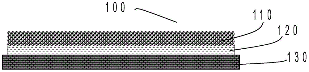
[0032] See figure 1 , figure 1 It is a schematic structural diagram of Embodiment 1 of the wavelength conversion device of the present invention. As shown in the figure, the wavelength conversion device 100 includes a substrate 130 , a light emitting layer 110 , and a reflective layer 120 . Wherein, the reflective layer 120 includes reflective particles, auxiliary particles and a first binder, and the light emitting layer 110 includes a wavelength conversion material and a second binder.

[0033] As described in the background technology, the light emitted by the light-emitting layer is incident on the reflective layer, and is reflected back to the light-emitting layer. The heat generated by the light-emitting layer is conducted to the substrate through the reflective layer, and then dissipated.

[0034] In the wavelength conversion device 100, the reflective layer 120 has two functions, one is light reflection, and the other is heat conduction. The reflective layer 120 need...

Embodiment 2

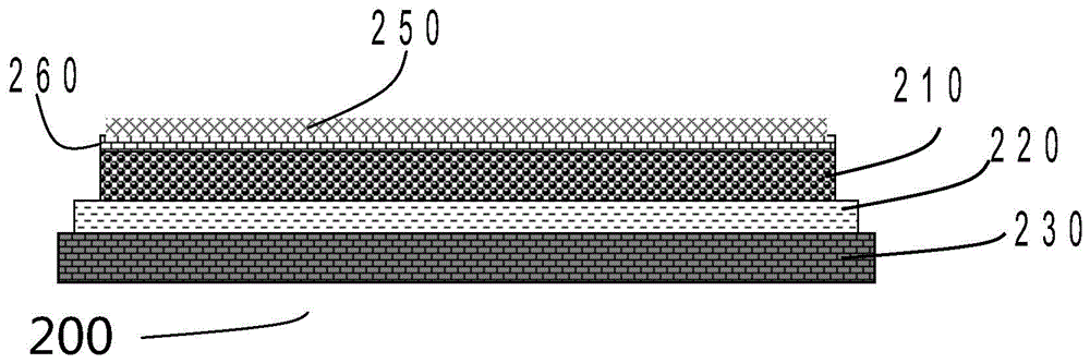
[0056] See figure 2 , figure 2 It is a schematic structural diagram of Embodiment 2 of the wavelength conversion device of the present invention. The light-emitting layer 210 , the reflective layer 220 and the substrate 230 in the wavelength conversion device 200 of this embodiment are the same as those in Embodiment 1, and details will not be repeated in this embodiment. The difference from Example 1 is that, if figure 2 As shown, the wavelength conversion device 200 further includes a glass layer 260 and an antireflection film 250 .

[0057] The glass layer 260 is located on the light emitting layer 210 and is composed of a third glass frit. Since there may be a small amount of wavelength conversion material particles protruding from the surface of the luminescent layer 210, coating on this surface may cause unevenness of the film layer, and if the luminescent layer is polished and then coated, the luminescent layer may be damaged during the grinding and polishing proc...

Embodiment 3

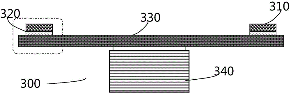
[0061] See image 3 , image 3It is a structural schematic diagram of Embodiment 3 of the wavelength conversion device of the present invention. The light-emitting layer 310 , the reflective layer 320 and the substrate 330 in the wavelength conversion device 300 of this embodiment are the same as those in Embodiment 1, and details will not be repeated in this embodiment. Different from Embodiment 1, this embodiment further includes a driving device 340, specifically, the driving device 340 in this embodiment is a motor. The substrate 330 in this embodiment is a circular substrate, carrying a circular reflective layer 320 and a light emitting layer 310 . The driving device 340 is fixedly connected with the substrate 330. When the driving device 340 rotates, it drives the substrate 330, the reflective layer 320 and the luminescent layer 310 on it to rotate together, so as to prevent the excitation light of the excitation light source from irradiating a point on the luminescent...


PUM

PropertyMeasurementUnit
particle diameteraaaaaaaaaa

Abstract

The invention discloses a wavelength conversion device and a related light emitting device thereof. The wavelength conversion device comprises a substrate, a reflecting layer and a light emitting layer which are superimposed in sequence. The light emitting layer contains a wavelength conversion material and a second binder. The reflecting layer contains reflecting particles, auxiliary particles and a first binder, wherein the reflecting particles are used for reflecting light, the auxiliary particles are used for filling the gaps of the reflecting particles, and the first binder is used for binding the reflecting particles and the auxiliary particles into a layer. The reflecting layer not only ensures high reflectivity, but also achieves small thickness. Therefore, heat generated by the light emitting layer can be better transferred to the substrate through the reflecting layer, and reduction of light conversion efficiency due to too high temperature of the light emitting layer is avoided.

Description

technical field [0001] The invention relates to the fields of display and lighting, in particular to a wavelength conversion device and a related light emitting device. Background technique [0002] With the development of display and lighting technology, the original LED or halogen bulb as a light source is increasingly unable to meet the high power and high brightness requirements of display and lighting. Visible light of various colors can be obtained by using excitation light emitted by a solid-state light source such as LD (Laser Diode, laser diode) to excite wavelength conversion materials, and this technology is increasingly used in lighting and display. This technology has the advantages of high efficiency, low energy consumption, low cost, and long life, and is an ideal alternative to existing white or monochromatic light sources. [0003] In the prior art, in order to improve the light utilization rate, the light sources of laser-excited wavelength-converting mate...

Claims


Application Information

Patent Timeline
Patent Type & Authority Applications(China)
IPC IPC(8): H01S5/06F21V9/40
CPCF21V13/08F21V7/24F21V9/30G02B5/0284G02B5/0294C09J1/02C09J11/02C09J183/00F21S8/00F21V7/22F21V13/04F21K9/64F21Y2115/30F21V9/40G02B1/11G02B5/0257H05K1/05B32B15/08C08K3/22C08K2003/2227C08K2003/2241
Inventor 李乾许颜正田梓峰陈雨叁
Owner APPOTRONICS CORP LTD
Why Eureka
Try Eureka