Chip automatization test system

An automated test and chip technology, applied in the field of microelectronics, can solve problems such as difficult maintenance of programs, poor signal quality, and error-prone programs, and achieve the effects of avoiding poor signal quality, easy maintenance, and saving time

Inactive Publication Date: 2016-02-17
KTMICRO ELECTRONICS
View PDF5 Cites 9 Cited by
  • Summary
  • Abstract
  • Description
  • Claims
  • Application Information

AI Technical Summary

Problems solved by technology

[0012] However, the test system of the chip in the prior art needs to maintain the programs separately for the test programs that realize different test functions, and needs to program different test programs for each test, and the repeated program programming is prone to errors and consumes a lot of time. Time also makes the program not easy to maintain; and for the cascading of these multi-stage boards of test motherboard 14, chip adapter board 15 and chip board 16, the quality of the signal will be made poor

Method used


Image

  • Chip automatization test system
  • Chip automatization test system
  • Chip automatization test system

Examples


Embodiment Construction

[0041] The present invention will be further described below in conjunction with the accompanying drawings and specific embodiments.

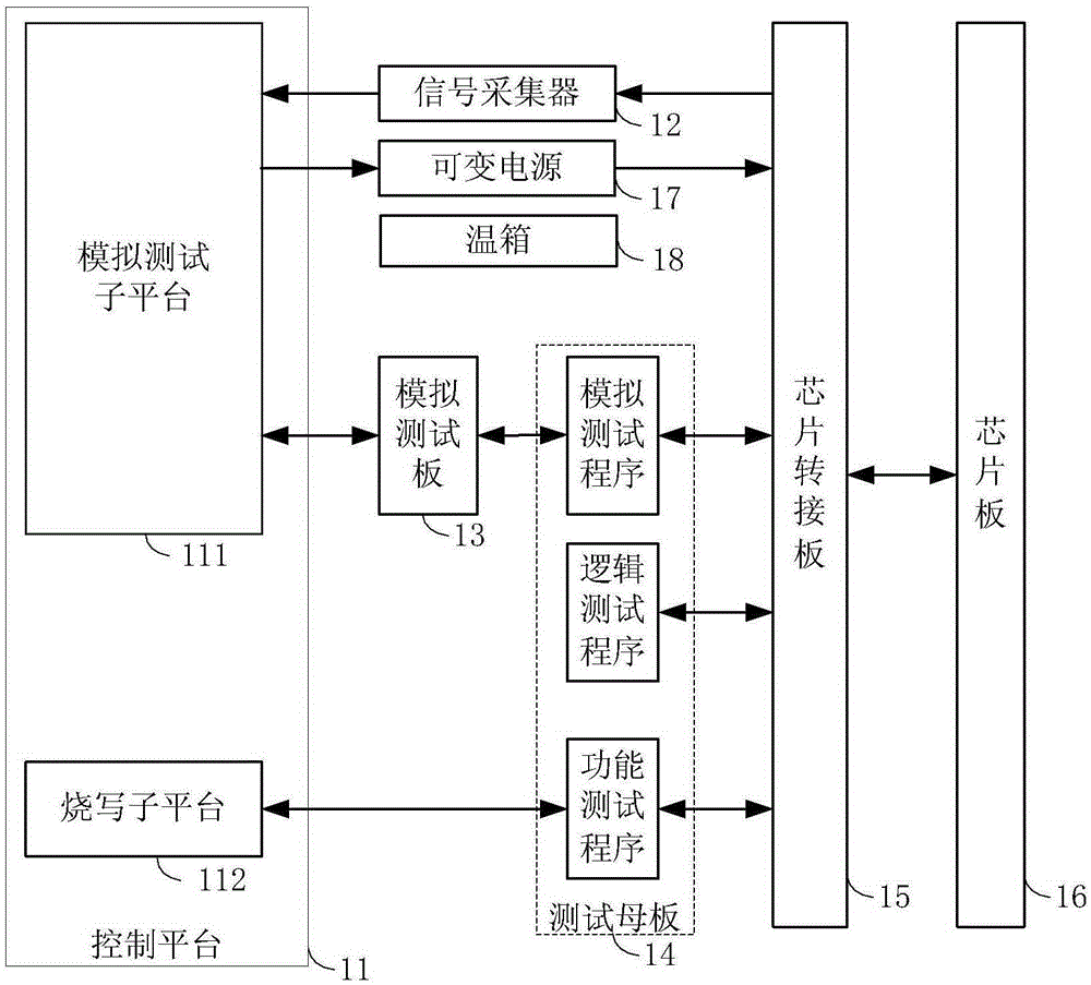
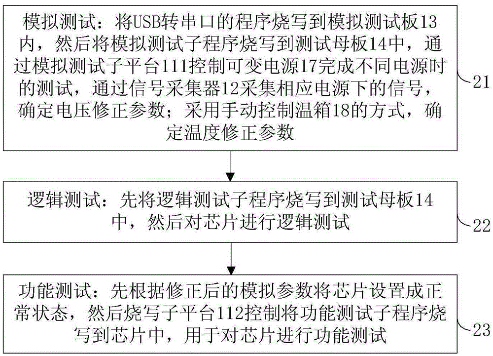
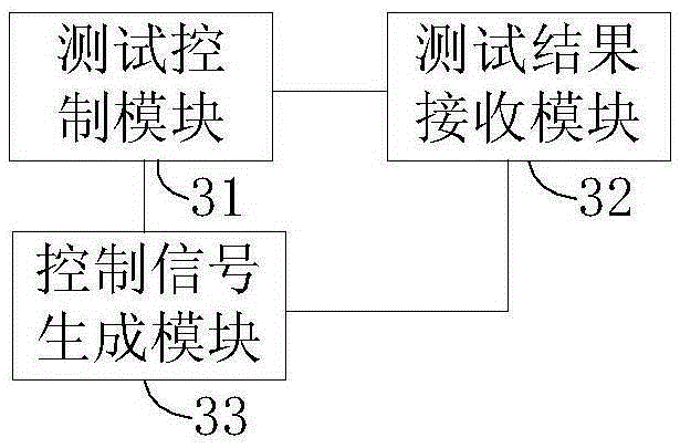
[0042] Such as image 3 Shown is a schematic structural diagram of an embodiment of an automatic test control device for chips according to the present invention. The automatic test control device may include: a test control module 31 and a test result receiving module 32 . Wherein, the test result receiving module 32 is connected with the test control module 31 .

[0043] In this embodiment, the test control module 31 is used to generate a test program selection command, and sends a test program selection command to the automated test board. The test program selection command is used to select a test subroutine from the automated test program. The automated test program includes two The above test subroutines, specifically, can generate an automated test program from different test programs; the test result receiving module 32 is used to rece...


PUM


Abstract

The invention relates to a chip automatization test system which comprises an automatization testing and controlling device for a chip, and an automatization test plate for the chip. The automatization testing and controlling device for the chip comprises a testing and controlling module and a test result receiving module, wherein the testing and controlling module is used for generating a test program selection command, sending the test program selection command to an automatization test plate, and the test program selection command is used for selecting a test subprogram from the automatization test program and the automatization test program comprises more than two test subprograms; the test result receiving module is used for receiving a test result sent by the automatization test plate. The system avoids repeatedly programming different test programs, so that the system avoids the mistake during testing, saves time, is easy to maintain, reduces the cascading between the plates, and avoids the situation of the poor signal quality caused by the cascading between multilevel plates.

Description

technical field [0001] The invention relates to the field of microelectronics, in particular to a chip automatic testing system. Background technique [0002] The chip needs to go through many links from design to processing and manufacturing, and then to packaging, which brings great challenges to the chip testing work and increases the complexity of the chip testing work. Typically, different tests are required on the chip, which requires several different test programs. During the testing process of the chip, it is necessary to select the required test program from different test programs through a test platform, and then burn the selected test program into the corresponding test motherboard through the programming platform, and the test motherboard transfers the test program through the chip. The connecting board is connected with the chip board, and then the test program is run for testing. After several rounds of such operations, the testing of the chip is completed. ...

Claims


Application Information

Patent Timeline
Patent Type & Authority Applications(China)
IPC IPC(8): G01R31/28
Inventor 孙马秋王晓玲杨芬
Owner KTMICRO ELECTRONICS
Why Eureka
Try Eureka