Silicon wafer transmission control method and system

A transmission control and silicon wafer technology, which is applied in the field of silicon wafer transmission control methods and systems, can solve problems affecting yield, silicon wafer pollution, transmission cavity occupation, etc., and achieves the effect of eliminating waiting time and avoiding pollution

Active Publication Date: 2016-02-17
BEIJING NAURA MICROELECTRONICS EQUIP CO LTD
View PDF4 Cites 11 Cited by
  • Summary
  • Abstract
  • Description
  • Claims
  • Application Information

AI Technical Summary

Problems solved by technology

[0004] In the case of a long process time, this transmission method will cause that there may be processed or unprocessed silicon wafers waiting to be transmitted in each module of the machine.
If the silicon wafer is waiting in the machine for a long time, on the one hand, the residual particles in the machine will cause some unnecessary pollution to the silicon wafer and affect the yield; on the other hand, it will also cause the transmission chamber to be occupied. During scheduling, transmission cannot be performed, which reduces transmission efficiency

Method used


Image

  • Silicon wafer transmission control method and system
  • Silicon wafer transmission control method and system
  • Silicon wafer transmission control method and system

Examples


Embodiment Construction

[0042] The silicon wafer transmission control method and system provided by the embodiments of the present invention will be described below with reference to the accompanying drawings.

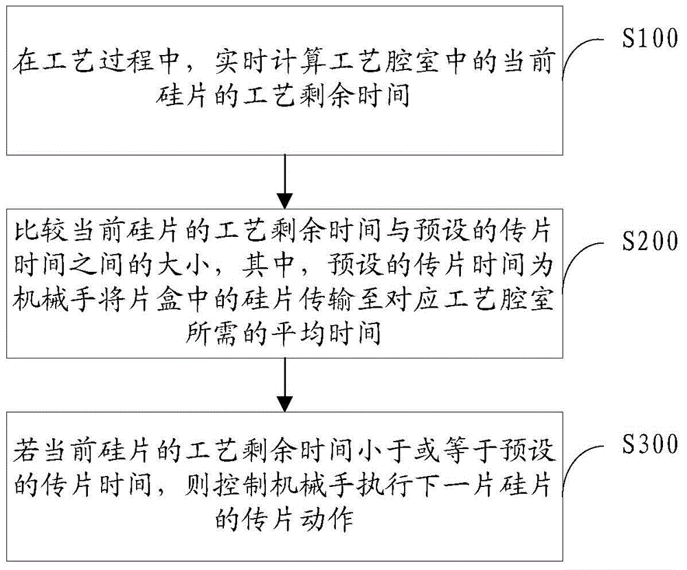
[0043] see figure 1 , the silicon wafer transmission control method provided by the present invention, comprises the following steps:

[0044] S100, during the process, calculate the remaining process time of the current silicon wafer in the process chamber in real time;

[0045] S200, comparing the remaining time of the current silicon wafer process with the preset film transfer time, wherein the preset film transfer time is the average time required for the robot to transfer the silicon wafers in the cassette to the corresponding process chamber ;

[0046] S300, if the remaining process time of the current silicon wafer is less than or equal to the preset wafer transfer time, control the manipulator to execute the wafer transfer action of the next silicon wafer.

[0047] The remaining ti...


PUM


Abstract

The invention discloses a silicon wafer transmission control method and system. The method includes the following steps that: in a processing process, the processing remaining time of a current silicon wafer in a processing chamber is computed in real time; the processing remaining time of the current silicon wafer is compared with preset wafer transfer time, wherein the preset wafer transfer time is mean time required by a manipulator to transfer silicon wafers in a wafer box to corresponding processing chambers; and if the processing remaining time of the current silicon wafer is smaller than the preset wafer transfer time, the manipulator is controlled to execute a wafer transfer action of the next silicon wafer. With the silicon wafer transmission control method and system of the invention adopted, waiting time of the silicon wafers in transfer chambers can be decreased or even eliminated, and therefore, pollution to the silicon wafers caused waiting can be avoided, and therefore, the transfer efficiency of the silicon wafers and the yield of a machine can be improved.

Description

technical field [0001] The invention relates to the field of semiconductor manufacturing, in particular to a silicon wafer transmission control method and system. Background technique [0002] In a semiconductor manufacturing plant, when performing an etching process on a silicon wafer, the silicon wafer needs to be transported between various modules of the machine according to a preset path. Usually, the transmission path of silicon wafers is: cassette (LoadPort, LP for short), atmospheric manipulator, transmission chamber (LoadLock, LL for short), vacuum manipulator, process chamber (ProcessModule, PM for short), vacuum manipulator, transmission chamber, atmosphere Manipulator, film box. [0003] In the process of silicon wafer transfer, in order to ensure that the entire process is completed with better efficiency, the control system judges that as long as there is a movable path, the robot arm will transfer the wafer. For example, while the first silicon wafer is bein...

Claims


Application Information

Patent Timeline
Patent Type & Authority Applications(China)
IPC IPC(8): H01L21/677
Inventor 刘振华
Owner BEIJING NAURA MICROELECTRONICS EQUIP CO LTD
Why Eureka
Try Eureka