Polysilicon array substrate manufacturing method, polysilicon array and display panel

A technology of an array substrate and a manufacturing method, which is applied in the display field, can solve the problems of difficulty in manufacturing and complicated manufacturing process of a polysilicon array substrate, and achieve the effect of reducing the difficulty of manufacturing and simplifying the manufacturing process.

Inactive Publication Date: 2016-02-17
BOE TECH GRP CO LTD
View PDF3 Cites 8 Cited by
  • Summary
  • Abstract
  • Description
  • Claims
  • Application Information

AI Technical Summary

Problems solved by technology

[0003] However, in the prior art, a polysilicon array substrate is made to form a light-shielding layer, an active layer, a gate (including a gate line), an interlayer insulating layer (including a gate insulating layer), a source / drain (including a data line), resin The patterns of the flat layer, the common electrode, the passivation layer, and the pixel electrode each require a patterning process, and a masking process is performed in one patterning process, that is to say, at least nine masking processes are required to make a polysilicon array substrate, so that The manufacturing process of the polysilicon array substrate is relatively complicated and difficult to manufacture

Method used


Image

  • Polysilicon array substrate manufacturing method, polysilicon array and display panel
  • Polysilicon array substrate manufacturing method, polysilicon array and display panel
  • Polysilicon array substrate manufacturing method, polysilicon array and display panel

Examples


Embodiment 1

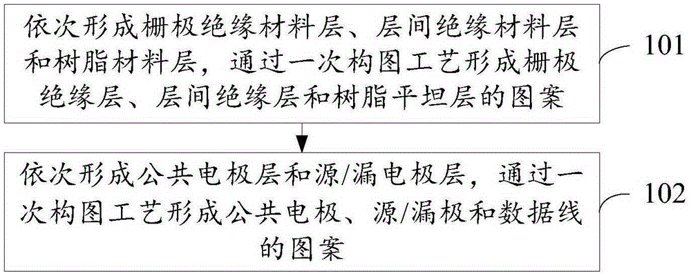
[0030] see figure 1 , the method for manufacturing a polysilicon array substrate provided by an embodiment of the present invention includes:

[0031] In step 101, a gate insulating material layer, an interlayer insulating material layer and a resin material layer are sequentially formed, and the patterns of the gate insulating layer 16, the interlayer insulating layer 18 and the resin flat layer 19 are formed through a patterning process; in this step, Form a layer of gate insulating material, form a layer of interlayer insulating material above the layer of gate insulating material, form a layer of resin material on the layer of interlayer insulating material, and use a patterning process to form the gate insulating layer 16, Patterns of the interlayer insulating layer 18 and the resin flat layer 19 .

[0032] In step 102, a common electrode layer and a source / drain electrode layer are sequentially formed, and the patterns of the common electrode 20, the source / drain electr...

Embodiment 2

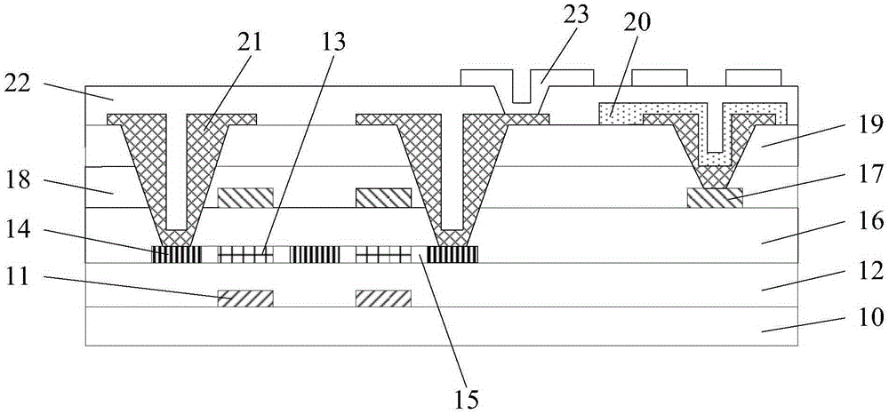
[0041] see Figure 5 , the specific implementation method of step 101 and step 102 in the first embodiment will be described below, wherein, step 101 can be specifically refined into step 1011 and step 1012, and step 102 can be specifically refined into step 1021-step 1024, and the specific content is as follows :

[0042] Step 1011, sequentially forming a gate insulating material layer, an interlayer insulating material layer and a resin material layer.

[0043] Step 1012: Perform an etching process on the resin material layer, the interlayer insulating material layer, and the gate insulating material layer by using a mask process, and form a first pass on the resin material layer, the interlayer insulating material layer, and the gate insulating material layer. hole and the second via hole to obtain the pattern of the resin planar layer 19, the interlayer insulating layer 18 and the gate insulating layer 16; wherein, the first via hole penetrates the resin material layer, t...

Embodiment 3

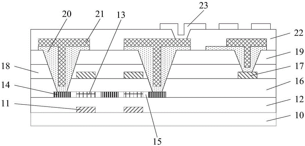
[0051] see Image 6 , in the polysilicon array substrate, it also includes a base substrate 10, a light shielding layer 11, an active layer 13, an ohmic contact layer 14, a lightly doped drain layer 15, a gate and a gate line 17, a passivation layer 22 and a pixel electrode 23 and other structures, in order to make the above structure, before step 101 in the first embodiment, also include step 103-step 105, after step 102, also include step 106 and step 107, the specific content of step 103-step 107 is as follows:

[0052] Step 103 , forming a light-shielding material layer on the base substrate 10 , and forming a pattern of the light-shielding layer 11 through one patterning process.

[0053] Step 104 , forming an active material layer on the light shielding layer 11 and the base substrate 10 , and forming a pattern of the active layer 13 through a patterning process.

[0054] In step 105, a gate electrode layer is formed on the active layer 13, and the pattern of the gate a...


PUM


Abstract

The invention discloses a polysilicon array substrate manufacturing method, a polysilicon array and a display panel, relating to the display technology field. The invention solves the problem that the manufacture method for the polysilicon array substrate is complicated and is difficult. The polysilicon array substrate manufacturing method comprises steps of successively forming a grid material insulation layer, an interlayer insulation material layer and a resin material layer, forming the patterns of the grid insulation layer, the interlayer insulation layer and a resin flat layer through one-time technical drawing, and/or, successively forming a public electrode layer and a source/drain electrode layer, and forming the patterns of the public electrode, the source/drain electrode and the data line through one time technical drawing. The polysilicon array substrate is obtained through the polysilicon array substrate manufacturing method, and the display panel comprises the polysilicon array substrate provided by the technical scheme. The polysilicon array substrate manufacturing method is used for manufacturing the polysilicon array substrate.

Description

technical field [0001] The invention relates to the field of display technology, in particular to a method for manufacturing a polysilicon array substrate, a polysilicon array substrate and a display panel. Background technique [0002] At present, with the rapid development of electronic equipment, more and more display panels are used in electronic equipment. The display panel includes an array substrate and a color filter substrate, and the array substrate is one of the important components of the display panel. According to the material of the thin film transistors in the array substrate, the array substrate can be divided into a polysilicon array substrate and an amorphous silicon array substrate. The electron mobility of the polysilicon array substrate is much greater than that of the amorphous silicon array substrate. The greater advantage is that polysilicon array substrates are often obtained by low-temperature polysilicon technology. Low-temperature polysilicon tec...

Claims


Application Information

Patent Timeline
Patent Type & Authority Applications(China)
IPC IPC(8): H01L21/77H01L27/12
CPCH01L27/1288H01L27/1214
Inventor 孙双张斌
Owner BOE TECH GRP CO LTD
Why Eureka
Try Eureka