Inversion multijunction solar cell chip of integration bypass diode and preparation method thereof

A technology of multi-junction solar cells and bypass diodes, applied in diodes, circuits, photovoltaic power generation, etc., can solve the problem that high-current batteries cannot realize the integration of bypass diodes, and achieve the effect of reducing battery weight and improving heat dissipation

Active Publication Date: 2016-02-17
TIANJIN SANAN OPTOELECTRONICS
View PDF4 Cites 5 Cited by
  • Summary
  • Abstract
  • Description
  • Claims
  • Application Information

AI Technical Summary

Problems solved by technology

[0003] In view of the above problems, the present invention provides a flip-chip multi-junction solar cell chip with integrated bypass diode and its preparation method. The bypass diode is arranged on the back of the cell chip, and its electrodes are also located on the back of the cell, so that the effective illumination area is reduced. Zero waste, and since the bypass diode is on the non-light-receiving side of the battery, there is no limit to its area size, which solves the problem that the bypass diode cannot be integrated in a high-current battery

Method used


Image

  • Inversion multijunction solar cell chip of integration bypass diode and preparation method thereof
  • Inversion multijunction solar cell chip of integration bypass diode and preparation method thereof
  • Inversion multijunction solar cell chip of integration bypass diode and preparation method thereof

Examples


Embodiment

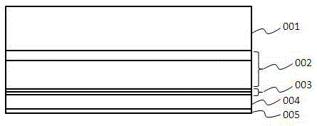
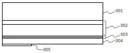
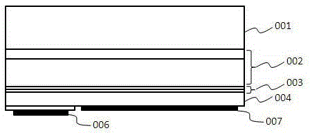
[0032] Such as figure 1 As shown, a flip-chip grown multi-junction solar cell epitaxial wafer is provided, and its structure includes: an epitaxial substrate 001, an n / p photoelectric conversion layer 002, a p / n tunnel junction 003, a bypass diode structure n-type layer 004, and a p type layer 005, wherein the n-type layer of the n / p photoelectric conversion layer 002 is used as the emission region and grown on the epitaxial substrate 001, and the p-type layer is used as the base region and grown on the n-type layer, p / n The tunnel junction 003 is grown on the p-type layer of the photoelectric conversion layer 002, the bypass diode n-type layer 004 is grown on the p / n tunnel junction 003 with a thickness of 3 μm, and the bypass diode p-type layer 005 is grown on the n Type layer 004, with a thickness of 50nm, the photoelectric conversion layer 002 also includes a window layer on the upper surface of the n-type layer, and a back field layer on the lower surface of the p-type la...


PUM


Abstract

The invention discloses an inversion multijunction solar cell chip of an integration bypass diode and a preparation method thereof. The solar cell chip comprises from top to down a glass cover sheet, a transparent bonding layer, a front electrode, an n/p photoelectric conversion layer, a p/n tunneling junction, an n/p bypass diode structure layer, a first back electrode, a second back electrode and at least one through hole. The p-type layer of the n/p bypass diode structure layer is partially etched and parts of n-type layer are exposed. The first back electrode covers but does not exceed the n/p bypass diode structure layer. The second back electrode covers but does not exceed the exposed n-type layer of the n/p bypass diode structure layer. The through holes penetrate the n/p photoelectric conversion layer, the p/n tunneling junction and the n/p bypass diode structure layer. An electric insulating layer is deposed on the inner wall of each of the through holes. The through holes are filled with metal connecting the front electrode and the first back electrode. According to the invention, effective light accepting area of the cell chip will not be occupied; a substrate-free ultrathin cell is achieved; heat dissipation ability of the cell is greatly improved; and due to the quite light weight, the solar cell chip has outstanding advantages in space power supply application.

Description

technical field [0001] The invention relates to a flip-chip multi-junction solar battery chip integrated with bypass diodes and a preparation method thereof, belonging to the field of semiconductor optoelectronic devices and technologies. Background technique [0002] Solar cells are one of the most important clean energy sources. Due to the dispersion of solar energy, a large-scale power supply system must use a large number of solar cells for series-parallel connection. The resulting problem is that once one of the cells in the series-parallel network If the cell fails, the power generation power of the entire network will drop significantly. At the same time, the failed cell is equivalent to a load, forming a so-called hot spot. Under a long-term load, the failed cell will be irreversibly damaged, that is, the entire network will be affected by irreversible efficiency. Attenuation, or even the failure of the entire network. Therefore, a reverse diode is usually connected...

Claims


Application Information

Patent Timeline
Patent Type & Authority Applications(China)
IPC IPC(8): H01L27/142H01L31/0224H01L21/82
CPCH01L21/82H01L27/1421H01L31/022441H01L31/0224H01L31/022433H01L31/1896H01L31/0443H01L31/0445Y02E10/544Y02E10/547Y02P70/50H01L31/048H01L31/0687H01L31/1892Y02E10/50
Inventor 熊伟平毕京锋陈文浚刘冠洲杨美佳李明阳吴超瑜王笃祥
Owner TIANJIN SANAN OPTOELECTRONICS
Why Eureka
Try Eureka