ESD (electro-static discharge) structure of trench type MOSFET and technological method

A process method and trench-type technology, applied in the field of ESD structure of trench-type MOSFET, can solve problems such as restricting gate PAD area, and achieve the effects of reducing deposition and etching steps, simplifying process steps, and reducing costs

Active Publication Date: 2016-02-24
SHANGHAI HUAHONG GRACE SEMICON MFG CORP
View PDF2 Cites 13 Cited by
  • Summary
  • Abstract
  • Description
  • Claims
  • Application Information

AI Technical Summary

Problems solved by technology

ESD polysilicon is usually located under the gate PAD, which restricts the area of ​​the gate PAD

Method used


Image

  • ESD (electro-static discharge) structure of trench type MOSFET and technological method
  • ESD (electro-static discharge) structure of trench type MOSFET and technological method
  • ESD (electro-static discharge) structure of trench type MOSFET and technological method

Examples


Embodiment Construction

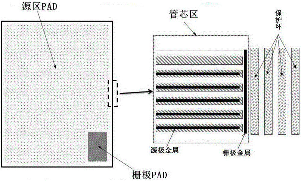
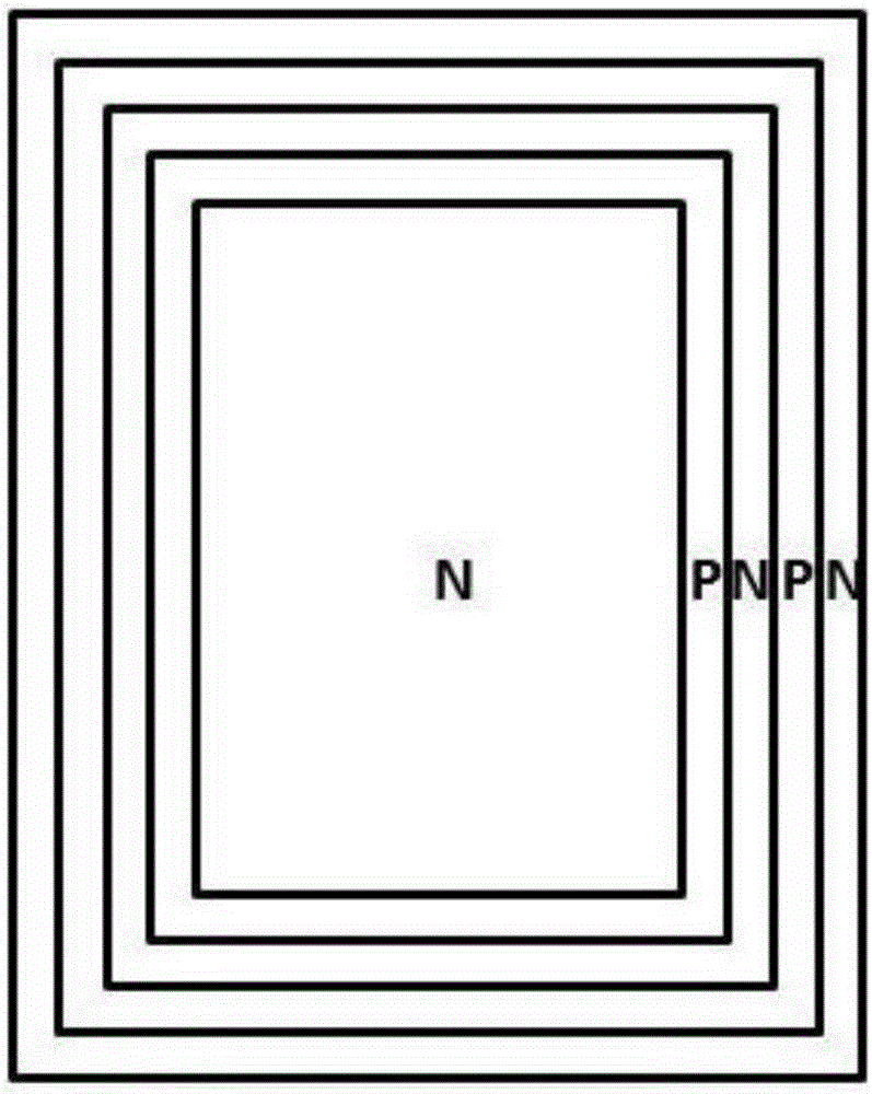
[0036] The ESD structure of trench type MOSFET described in the present invention, as Figure 6 As shown, it includes: there is a guard ring trench around the trench MOSFET, the ESD structure is integrated in the guard ring trench, the guard ring trench passes through the bottom of the body region and is located in the epitaxial layer, and the trench Filled with polysilicon;

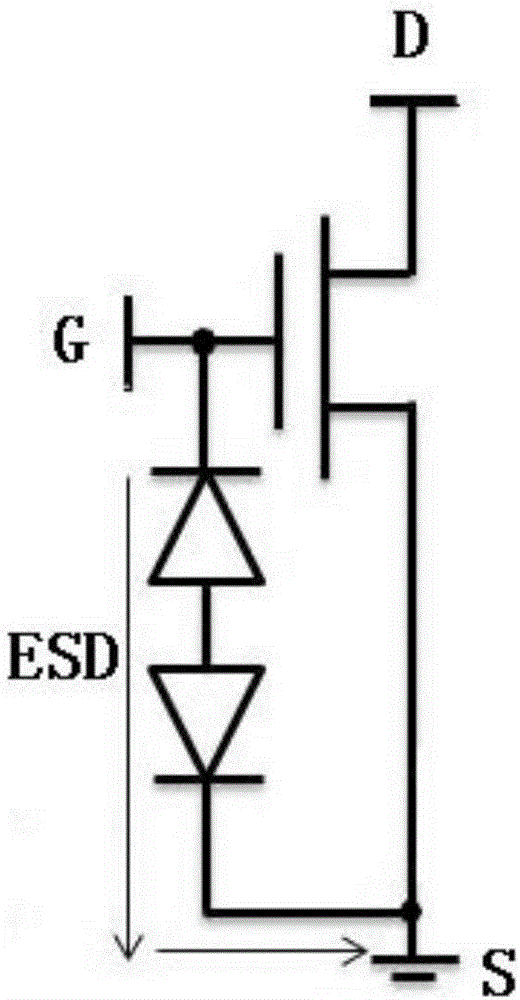
[0037] The polysilicon segment is doped with N-P or P-N, or N-P-...-N-P or P-N-...-P-N interval doping to form one or more equivalent series diodes, the structure of which is as follows Figure 7 Shown is a schematic cross-sectional view of the ESD protection ring trench. Electrodes at both ends of the series-connected diodes are respectively connected to the gate and the source of the trench MOSFET. Such as Figure 6 Among them, the trenches of the multi-layer protection ring are led out through the common electrodes 7 and 8, and are connected to the gate and source of the MOSFET by metal to form an ...


PUM


Abstract

The invention discloses an integrated ESD (electro-static discharge) structure of a trench type MOSFET; a trench type protective ring is arranged around the trench type MOSFET; the ESD structure is integrated in a protective ring trench; the protective ring trench passes through the bottom of a body region to be positioned in an epitaxial layer; the trench is filled with polycrystalline silicon; the polycrystalline silicon is subjected into interval doping in subsections of N-P or P-N, or N-P- until -N-P or P-N- until -P-N to form one or more equivalently concatenated diodes; and the electrodes in the first ends and the tail ends of the concatenated diodes are connected with the grid electrode and the source electrode of the trench type MOSFET respectively. According to the ESD structure of the trench type MOSFET, the polycrystalline silicon, with the alternatively-arranged Ns and Ps at intervals, is formed in the protective ring trench to equivalently form the ESD diodes; the two electrodes of the equivalent ESD diodes formed by PN junctions are connected with the source electrode and the grid electrode of the MOSFET respectively through metal leads to form the ESD protection structure of the MOSFET. According to the technological method for the ESD structure of the trench type MOSFET, by the adoption of the protective ring, the procedures of ESD polycrystalline silicon depositing and etching are reduced, so that the processing steps are simplified and the cost is reduced.

Description

technical field [0001] The invention relates to the field of semiconductor integrated circuit manufacturing, in particular to an ESD structure of a trench MOSFET, and also relates to a process method of the ESD structure of the trench MOSFET. Background technique [0002] ESD (Electro-Static Discharge) means "electrostatic discharge". ESD is a discipline formed since the middle of the 20th century to study the generation, harm and protection of static electricity. Therefore, it is customary in the world to refer to the equipment used for electrostatic protection as ESD, and the Chinese name is electrostatic impedance. Static electricity is an objectively existing natural phenomenon, which can be produced in many ways, such as contact, friction, induction between electrical appliances, etc. Static electricity is characterized by long-term accumulation, high voltage, low power, small current and short action time. [0003] The action of the human body or the contact, separa...

Claims


Application Information

Patent Timeline
Patent Type & Authority Applications(China)
IPC IPC(8): H01L27/02H01L21/82
CPCH01L21/82H01L27/0255H01L27/0296
Inventor 陈正嵘
Owner SHANGHAI HUAHONG GRACE SEMICON MFG CORP
Why Eureka
Try Eureka