Preparation method for vertical III-V family antimonide semiconductor monocrystalline thin film

A III-V, single-crystal thin-film technology, applied in semiconductor/solid-state device manufacturing, nanotechnology for materials and surface science, electrical components, etc., can solve the problem of no buffer layer, increased lattice dislocation, lattice relaxation Incomplete and other problems, to achieve the effect of easy device processing, high crystal quality, and save production costs

Active Publication Date: 2016-03-16
INST OF SEMICONDUCTORS - CHINESE ACAD OF SCI
View PDF5 Cites 7 Cited by
  • Summary
  • Abstract
  • Description
  • Claims
  • Application Information

AI Technical Summary

Problems solved by technology

However, in the buffer layer with continuously graded composition, dislocations are easier to extend upward along the epitaxial layer, even to the surface of the buffer layer, so that the surface of the buffer layer cannot form a perfect lattice structure, thus affecting the crystal quality of the epitaxial material
In addition, the compo...

Method used


Image

  • Preparation method for vertical III-V family antimonide semiconductor monocrystalline thin film

Examples


preparation example Construction

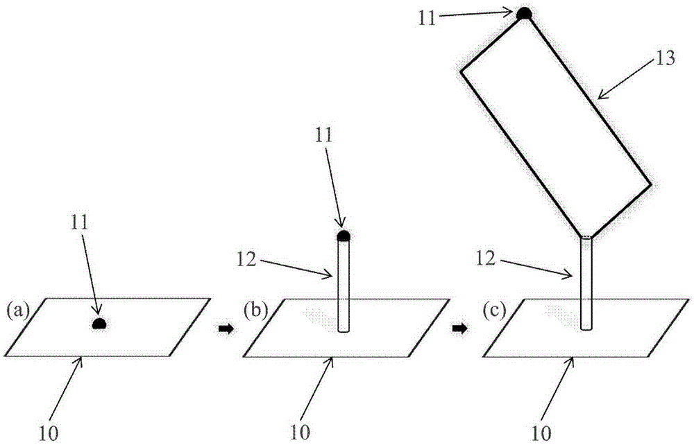
[0013] see figure 1 As shown, the present invention provides a method for preparing a vertical III-V group antimonide semiconductor single crystal thin film, comprising the steps of:

[0014] Step (a): preparing a plurality of metal catalyst particles 11 on the semiconductor substrate 10, the purpose of the metal catalyst particles 11 is to catalyze the growth of the III-V group semiconductor nanowire 12 in the catalytic step (b), and its material is Au, Ag, Cu, Pd, Mn, Ga or Fe, which are obtained by annealing corresponding metal thin films, have a diameter of several nanometers to hundreds of nanometers. The density of the metal catalyst particles 11 determines the density of the III-V semiconductor nanowires 12 in step (b), which can be adjusted by increasing or decreasing the thickness of the metal film or increasing or decreasing the annealing temperature of the metal film. The material of the semiconductor substrate 10 is Si, GaAs, GaSb, InAs, InSb, InP or GaP. The sem...

Embodiment 1

[0017] Embodiment 1: the preparation method of vertical InSb single crystal film

[0018] The invention provides a method for preparing a vertical III-V group antimonide semiconductor single crystal thin film, comprising the following steps:

[0019] Step (a): Using molecular beam epitaxy, deposit an Ag film with a thickness of about 0.5-2 nm on a Si(111) substrate at room temperature; anneal the Ag film at a high temperature (600° C.) for 20 minutes to disperse the film Forming catalyst particles with a diameter of about several nanometers to about 100 nanometers, the catalyst particles are used to catalyze the growth of InAs nanowires in step (b);

[0020] Step (b): Using molecular beam epitaxy, on the Si(111) substrate, using Ag as a catalyst to catalyze and grow InAs nanowires. The InAs nanowire growth temperature is 380°C-530°C, and the As / In beam current ratio is 30-50. The InAs nanowire diameter is about several nanometers to 100 nanometers; different InAs nanowire di...

Embodiment 2

[0022] Example 2: Vertical InAs x Sb 1-x (0

[0023] The invention provides a method for preparing a vertical III-V group antimonide semiconductor single crystal thin film, comprising the following steps:

[0024] Step (a): Using molecular beam epitaxy, deposit an Ag film with a thickness of about 0.5-2 nm on a Si(111) substrate at room temperature; anneal the Ag film at a high temperature (600° C.) for 20 minutes to disperse the film Forming catalyst particles with a diameter of about several nanometers to about 100 nanometers, the catalyst particles are used to catalyze the growth of InAs nanowires in step (b);

[0025]Step (b): Using molecular beam epitaxy, on the Si(111) substrate, using Ag as a catalyst to catalyze and grow InAs nanowires. The InAs nanowire growth temperature is 380°C-530°C, and the As / In beam current ratio is 30-50. The InAs nanowire diameter is about several nanometers to 100 nanometers; different ...


PUM


Abstract

The invention provides a preparation method for a vertical III-V family antimonide semiconductor monocrystalline thin film. The preparation method comprises the steps that step (a): multiple metal catalyst particles used for catalyzing nanowire growth are prepared on a semiconductor substrate; step (b): growth of III-V family semiconductor nanowires is catalyzed on the semiconductor substrate by utilizing the metal catalyst particles, and the metal catalyst particles are arranged at the top end of the III-V family semiconductor nanowires; and step (c): epitaxy of the vertical III-V family antimonide semiconductor monocrystalline thin film is performed on the axial direction of the III-V family semiconductor nanowires so that preparation is completed. Mass production of the vertical III-V family antimonide semiconductor monocrystalline thin film can be easily realized by the preparation method so that production cost of the III-V family antimonide semiconductor monocrystalline thin film can be greatly saved.

Description

technical field [0001] The invention relates to a semiconductor material preparation technology, and mainly relates to a preparation method of a vertical III-V group antimonide semiconductor single crystal thin film. Background technique [0002] In the past few decades, integrated circuit technology based on SiCMOS technology has followed "Moore's Law" to increase the working speed of the chip, increase the integration level and reduce the cost by reducing the feature size of the device. The feature size of integrated circuits has shrunk from the micrometer scale to the nanometer scale. However, with the development of integrated circuit technology to 22nm technology node and below, Si integrated circuit technology is limited by a series of basic physical problems and process technology problems in terms of speed, power consumption, integration and reliability. Traditional SiCMOS Technology's use of "scaling down" to produce smaller, faster and cheaper logic and memory dev...

Claims


Application Information

Patent Timeline
IPC IPC(8): H01L21/02B82Y30/00B82Y40/00
CPCB82Y30/00B82Y40/00H01L21/02463H01L21/02513H01L21/02549H01L21/02598H01L21/02631
Inventor 潘东赵建华
Owner INST OF SEMICONDUCTORS - CHINESE ACAD OF SCI
Why Eureka
Try Eureka