Optical coupling bidirectional thyristor element

A technology of silicon components and optical coupling, applied in the direction of electrical components, semiconductor devices, circuits, etc., can solve the problems of short distance, difficulty in obtaining joint margin, and limitation of pad size, so as to ensure withstand voltage, eliminate bad conditions, and chip zoom out effect

Active Publication Date: 2016-03-16
SHARP KK
View PDF5 Cites 2 Cited by
  • Summary
  • Abstract
  • Description
  • Claims
  • Application Information

AI Technical Summary

Problems solved by technology

[0005] However, in the above-mentioned planar semiconductor element, two channels need to be formed, and a total of f

Method used


Image

  • Optical coupling bidirectional thyristor element
  • Optical coupling bidirectional thyristor element
  • Optical coupling bidirectional thyristor element

Examples


no. 1 approach

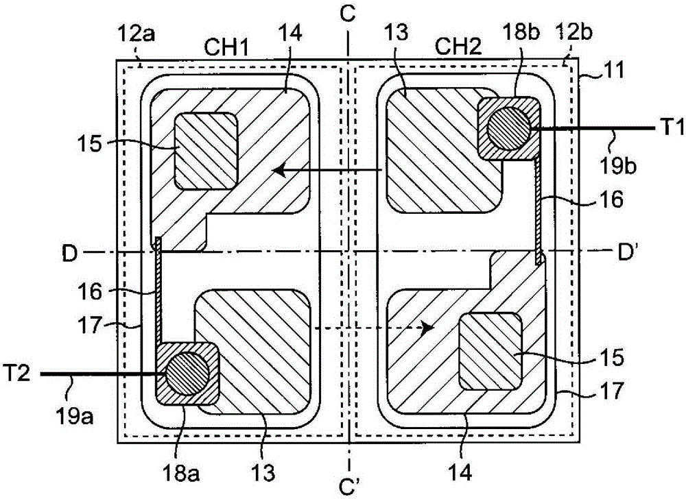
[0061] The optically coupled triac of this embodiment, and Figure 5 The shown optically coupled triac is likewise a point-symmetric optically coupled triac.

[0062] figure 1 A schematic pattern layout of the optically coupled triac of this embodiment is shown. Such as figure 1 As shown, the pattern has 180-degree rotational symmetry with respect to the intersection point of the center line C-C' and the line segment D-D' perpendicular to the center line in plan view, that is, a pattern that is substantially point-symmetrical with respect to the above-mentioned intersection point. Hereinafter, the photothyristor located on the left side of the figure with respect to the center line C-C' is called the photothyristor of CH1, and the photothyristor on the right side is called the photothyristor of CH2.

[0063] This optical coupling triac is composed of the first photothyristor 12 a of CH1 and the second photothyristor 12 b of CH2 formed separately on the surface of the N-typ...

no. 2 approach

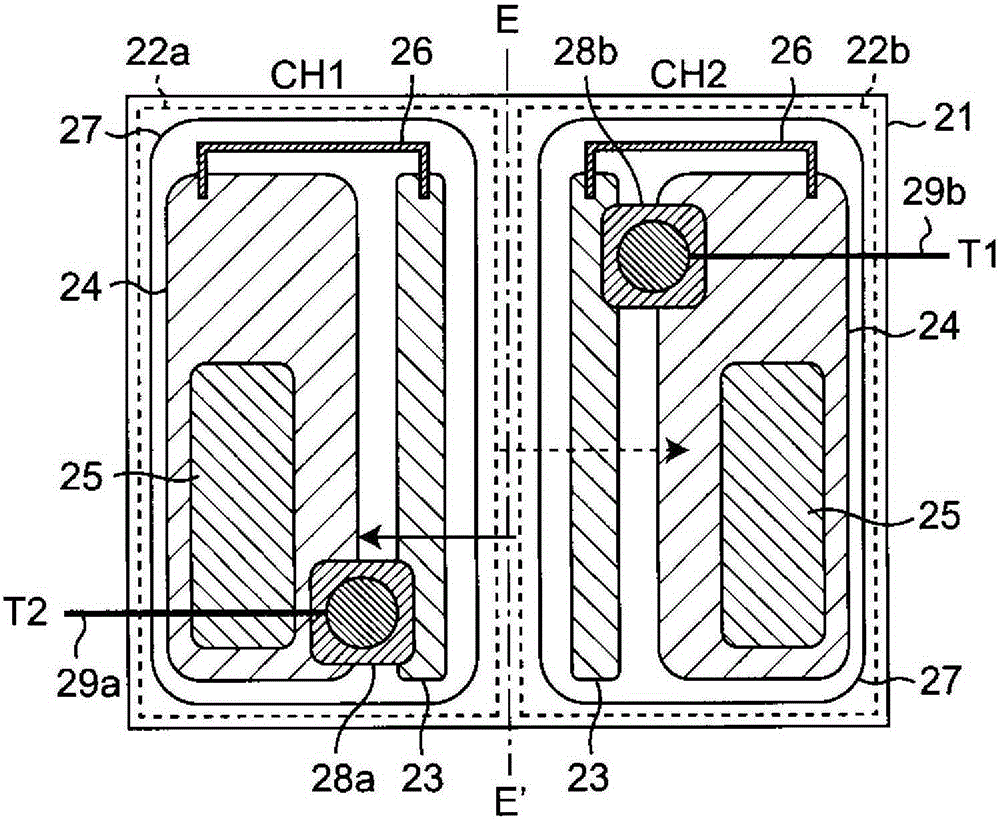
[0077] The optically coupled triac of this embodiment is a line object type optically coupled triac.

[0078] figure 2 A schematic pattern layout of the optically coupled triac of this embodiment is shown. Such as figure 2 As shown in , it has a substantially line-symmetrical pattern with respect to the center line E-E' in plan view. Hereinafter, the photothyristor located on the left side of the figure with respect to the center line E-E' is called the photothyristor of CH1, and the photothyristor on the right side is called the photothyristor of CH2.

[0079] The optical coupling triac is composed of the first photothyristor 22a of CH1 and the second photothyristor 22b of CH2 formed separately on the surface of the N-type silicon substrate 21 .

[0080] The first photosensitive thyristor 22a and the second photosensitive thyristor 22b respectively have: a P-type anode diffusion region 23 formed along the central line EE' on the central line EE' side; The P-type gate di...

no. 3 approach

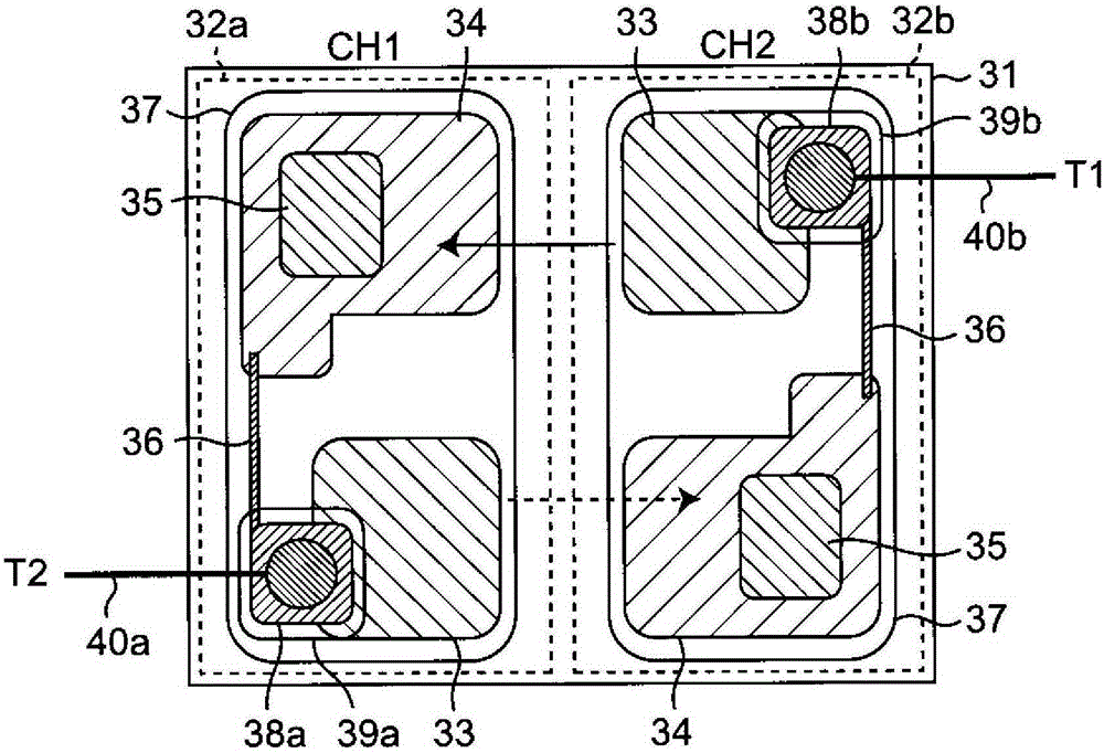
[0089] The optically coupled triac of the present embodiment is a point-symmetrical optically coupled triac similar to that of the above-described first embodiment.

[0090] image 3 The pattern layout of the optical coupling triac of this embodiment is shown. exist image 3 Among them, the N-type silicon substrate 31, the first photothyristor 32a of CH1, the second photothyristor 32b of CH2, the P-type anode diffusion region 33, the P-type gate diffusion region 34, the N-type cathode diffusion region 35, the high-resistance pattern 36. Al electrodes 37, pads 38a, 38b, Au wires 40a, 40b, and the N-type silicon substrate 11 in the first embodiment, the first photothyristor 12a of CH1, the second photothyristor 12b, P of CH2 Type anode diffusion region 13, P-type gate diffusion region 14, N-type cathode diffusion region 15, high resistance pattern 16, Al electrode 17, pads 18a, 18b, Au lines 19a, 19b are identical.

[0091] In addition, the operation of the optically coupled ...


PUM


Abstract

The invention provides an optical coupling bidirectional thyristor element capable realizing quality stabilization and chip reduction. The bidirectional thyristor element has a semiconductor chip which forms a first photosensitive thyristor portion (12a) and a second photosensitive thyristor portion (12b) which are mutually separated on a semiconductor substrate (11). Each photosensitive thyristor portion has a PNPN portion. The bidirectional thyristor element also has a joint bonding pad electrically connected to an anode diffusion region (13) and a cathode diffusion region (15) and insulated from a control electrode diffusion region (14). The PNPN portions of the first and second photosensitive thyristor portions (12a, 12b) are substantially point-symmetrically configured relative to a center of the semiconductor chip, or substantially line-symmetrically configured relative to a line segment passing through the center and in parallel to one side. The joint bonding pad (18a) of the first photosensitive thyristor portion (12a) and the joint bonding pad (18b) of a second photosensitive thyristor portion (12b) are mutually separately configured on one end side and the other end side of the above line segment in the extending direction.

Description

technical field [0001] The invention relates to a photocoupler triac (PHOTOTRIAL) element. Background technique [0002] Conventionally, as an optical coupling triac, there is a planar semiconductor element disclosed in JP-A-10-209431 (Patent Document 1). [0003] The planar semiconductor element has two channels composed of two anode regions, two gate regions, two cathode regions and two resistor regions on both sides of the substrate in a rectangular channel stop region. In this case, each of the above-mentioned anode regions is close to the above-mentioned channel stopper region (that is, outside the channel stopper region), each of the above-mentioned gate regions is formed between each of the above-mentioned anode regions and the central side of the above-mentioned substrate, and each of the above-mentioned The cathode region is formed outside the light entrance region of the optical signal in the above-mentioned gate region. [0004] Furthermore, the bonding pad on t...

Claims


Application Information

Patent Timeline
IPC IPC(8): H01L29/747
CPCH01L29/747
Inventor 冈本朋昭松本浩司
Owner SHARP KK
Why Eureka
Try Eureka