Packaging structure of light receiving/ transmitting sub module and manufacturing method thereof

A packaging structure and sub-module technology, applied in the coupling of optical waveguides, light guides, optics, etc., can solve the problems of large loss of product performance indicators, inability to adapt to batch operations, easy to break the fiber end, etc. Reliability guarantee, suitable for mass production, the effect of simplified overall structure

Active Publication Date: 2016-03-23
BROADEX TECH
View PDF3 Cites 18 Cited by
  • Summary
  • Abstract
  • Description
  • Claims
  • Application Information

AI Technical Summary

Problems solved by technology

Two optical fiber arrays are usually used in the traditional optical receiving sub-module. An optical fiber array is assembled at the input end of the arrayed waveguide grating chip, and then an optical fiber array is assembled at the output end of the arrayed waveguide grating chip and coupled with the array photodiode. Therefore, The structure is more complicated and the cost is higher; especially, the optical fiber array coupled with the photodiode array is exposed and easily broken and damaged, so the operability is relatively poor and cannot meet the needs of batch operation; and the use of two After the optical fiber array, the performance index loss of the product will increase
Similarly, one or more laser chips in the traditional light emitting sub-module need to be coupled to the optical fiber and then output. Multiple optical fibers are assembled into a fiber array and connected to the arrayed waveguide grating chip. The structure is also complex, the volume is large, and the operability is poor.

Method used


Image

  • Packaging structure of light receiving/ transmitting sub module and manufacturing method thereof
  • Packaging structure of light receiving/ transmitting sub module and manufacturing method thereof
  • Packaging structure of light receiving/ transmitting sub module and manufacturing method thereof

Examples


Embodiment Construction

[0027] Below in conjunction with specific embodiment, further illustrate the present invention. It should be understood that these examples are only used to illustrate the present invention and are not intended to limit the scope of the present invention. In addition, it should be understood that after reading the teachings of the present invention, those skilled in the art can make various changes or modifications to the present invention, and these equivalent forms also fall within the scope defined by the appended claims of the present application.

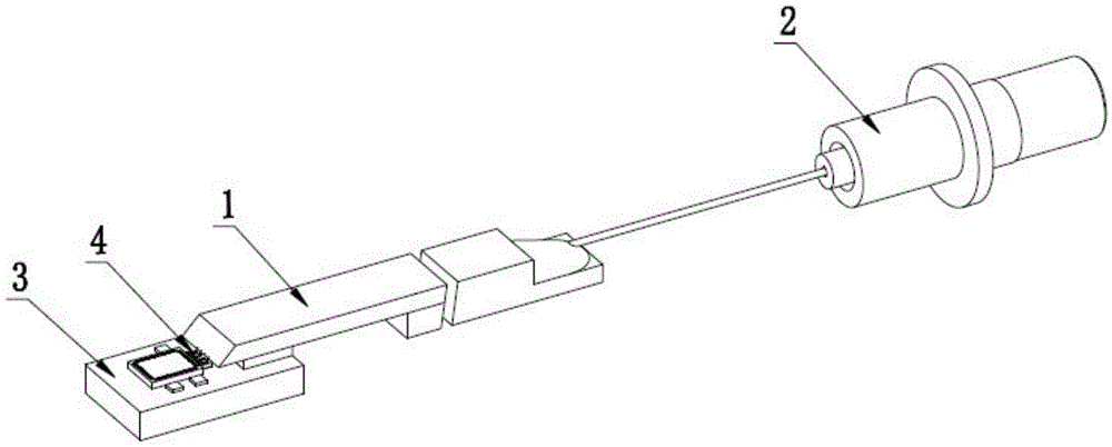
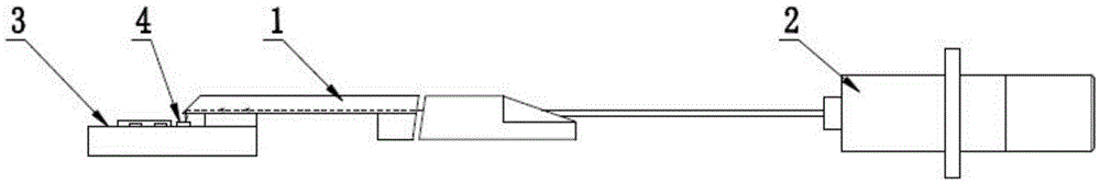
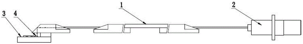
[0028] Embodiments of the present invention relate to a package structure of a light receiving / transmitting sub-module, such as figure 1 and figure 2 As shown, it consists of an arrayed waveguide grating chip 1, a fiber pigtail assembly 2 and a photoelectric / electro-optic conversion circuit board 3. The photoelectric / electro-optic conversion circuit board 3 is composed of an array photodiode or laser chip 4 and other correspo...


PUM


Abstract

The invention relates to a packaging structure of a light receiving / transmitting sub module. The packaging structure comprises an arrayed waveguide grating chip, an optical fiber pigtail assembly and a photo-electric / electro-optic conversion circuit board, wherein one end face of the arrayed waveguide grating chip is ground to form a ground angle of more than 10 degrees, and the photo-electric / electro-optic conversion circuit board is horizontally placed below the arrayed waveguide grating chip; and the optical fiber channel of the optical fiber pigtail assembly is correspondingly connected with a waveguide channel on the other end face of the arrayed plane waveguide grating chip through an optical fiber. One end face of the arrayed waveguide grating chip is machined to form a certain reflective angle and then directly coupled with an arrayed photo-electric diode or a laser chip on the photo-electric / electro-optic conversion circuit board to manufacture the light receiving / transmitting sub module, and only one optical fiber pigtail assembly is needed, so that the overall structure is simple, the loss is low and the cost is low; the process flow is simplified in the method of coupling with spatial light reflection, the operation is convenient, and the packaging structure is suitable for batch production.

Description

technical field [0001] The invention relates to a light receiving / transmitting sub-module in the field of optical fiber technology, in particular to a package structure of a light receiving / transmitting sub-module and a preparation method thereof. Background technique [0002] With the accelerated development of the Internet, cloud computing and big data industries, the huge demand for bandwidth from the growing IPTV and video game services is driving the development of broadband technology. High-speed and compact optical transceiver modules have become a common demand for optical communication equipment manufacturers and data centers. The optical receiving / transmitting sub-module (referred to as "ROSA / TOSA") is the core device in the optical transceiver module and has broad market prospects. [0003] The light receiving / transmitting sub-module is mainly assembled by arrayed waveguide grating chip, array photodiode or laser chip, input end and output end fiber pigtail assem...

Claims


Application Information

Patent Timeline
Patent Type & Authority Applications(China)
IPC IPC(8): G02B6/42
CPCG02B6/424G02B6/4287G02B6/4296
Inventor 丁勇闫超朱伟
Owner BROADEX TECH
Why Eureka
Try Eureka