Eureka AIR delivers breakthrough ideas for toughest innovation challenges, trusted by R&D personnel around the world.

Liquid crystal display panel, manufacturing method thereof and liquid crystal display device

A technology for liquid crystal display panels and liquid crystal display devices, which is applied in the directions of instruments, nonlinear optics, optics, etc., can solve the problems of light source waste, waste, light waste, etc., and achieve the effects of reducing product power consumption, increasing utilization, and avoiding waste.

Active Publication Date: 2016-03-23
SHANGHAI TIANMA MICRO ELECTRONICS CO LTD +1
View PDF8 Cites 9 Cited by
  • Summary
  • Abstract
  • Description
  • Claims
  • Application Information

AI Technical Summary

Problems solved by technology

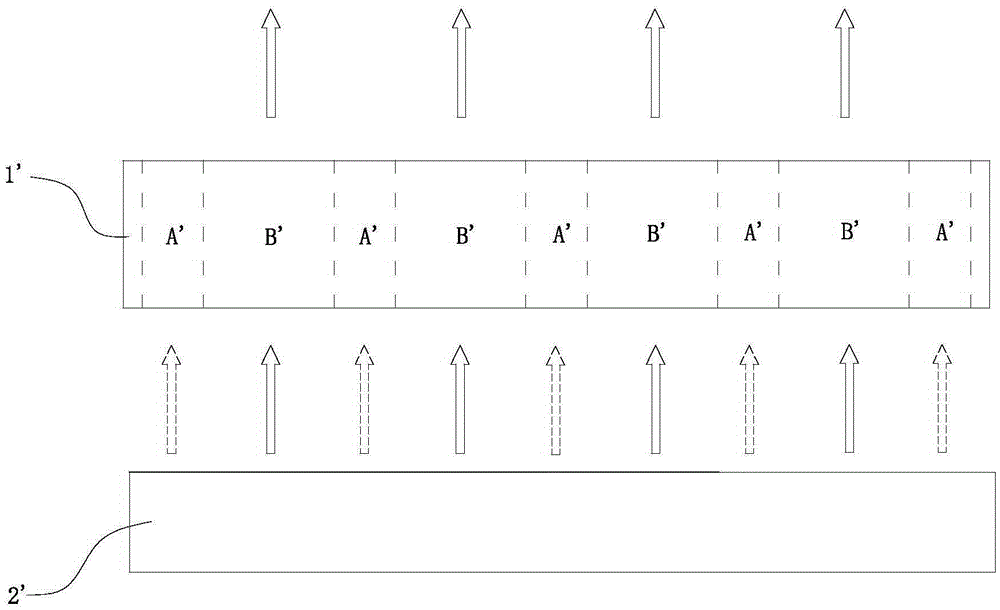
Depend on figure 1 It can be seen that among all the light incident on the incident side of the liquid crystal cell 1', only the light (i.e. figure 1 The arrow mark of the solid line in the center) can be emitted from the light-emitting side of the liquid crystal cell 1', and the light entering the light-shielding area A' of the liquid crystal cell 1' (i.e. figure 1 The arrow mark of the dotted line in the center) cannot be emitted from the light-emitting side of the liquid crystal cell 1', resulting in a waste of light in this part, especially when the aperture ratio of the pixel of a high-PPI product is already lower than 50%, the light in this part The waste of the liquid crystal display has led to problems such as energy utilization and low brightness.
[0005] The current liquid crystal display technology mainly improves energy utilization and brightness by increasing the pixel aperture ratio and improving the luminous efficiency of the backlight source, but there is no improvement in the shading area (ineffective display area), so that the radiation to the shading area The light in the (invalid display area) cannot be fully utilized, resulting in a lot of waste of light sources

Method used


Image

  • Liquid crystal display panel, manufacturing method thereof and liquid crystal display device
  • Liquid crystal display panel, manufacturing method thereof and liquid crystal display device
  • Liquid crystal display panel, manufacturing method thereof and liquid crystal display device

Examples


no. 1 example

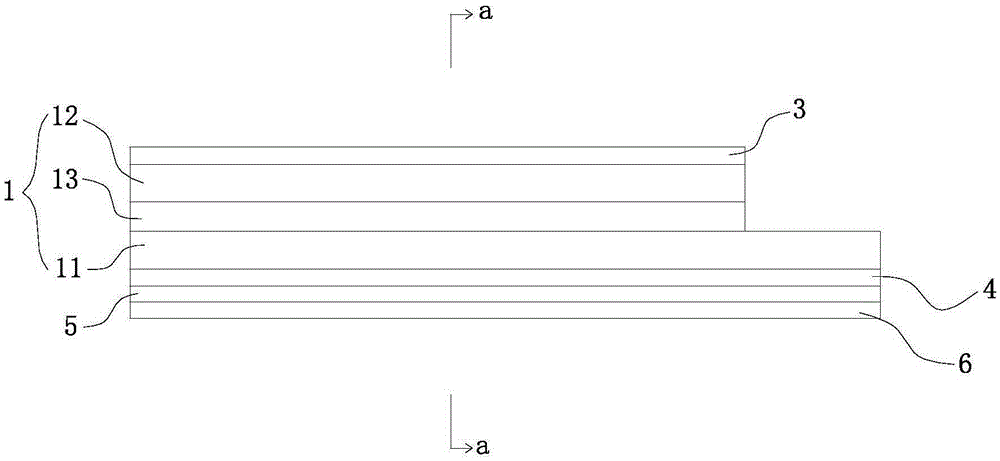
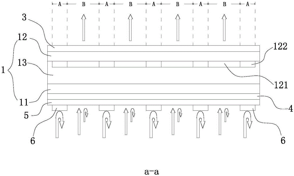
[0031] See figure 2 and image 3 , which respectively show a side view and a schematic cross-sectional structure of the liquid crystal display panel according to the first embodiment of the present invention. In an optional embodiment of the present invention, the liquid crystal display panel includes: a liquid crystal cell 1 , a first absorbing polarizing layer 3 , a second absorbing polarizing layer 4 , a reflecting polarizing layer 5 and a reflecting layer 6 .

[0032] The liquid crystal cell 1 includes a plurality of light-transmitting regions B (ie, the effective display region of the liquid crystal display panel) and a light-shielding region A surrounding each light-transmitting region B. Such as figure 2 As shown, the liquid crystal cell 1 includes: a first substrate 11 and a second substrate 12 oppositely arranged, and a liquid crystal molecule layer 13 arranged between the first substrate 11 and the second substrate 12 .

[0033]A sub-pixel array formed by a plur...

no. 2 example

[0064] The second embodiment of the present invention is another implementation mode of the liquid crystal display device of the present invention, Figure 12 A side view of the liquid crystal display device described in this embodiment is shown, including figure 2 and image 3 As shown in the liquid crystal display panel, backlight unit 2, drive unit 7 and flexible circuit board 8, optionally, the reflective layer 6 of the liquid crystal display panel in this embodiment is optionally made of a metal material, for example, the reflective layer 6 can be Made of silver, aluminum or their compounds. The difference from the liquid crystal display device described in the first embodiment is that the reflective layer 6 is grounded. Specifically, in Figure 12 In the illustrated embodiment, the reflective layer 6 is electrically connected to the flexible circuit board 8 disposed on the first substrate 11 through a conductive glue 81 . After the reflective layer 6 is electrically...

no. 3 example

[0066] The third embodiment of the present invention is another implementation mode of the liquid crystal display device of the present invention, Figure 13 A side view of the liquid crystal display device described in this embodiment is shown, including figure 2 and image 3 As shown in the liquid crystal display panel, backlight unit 2, drive unit 7 and flexible circuit board 8, optionally, the reflective layer 6 of the liquid crystal display panel in this embodiment is optionally made of a metal material, for example, the reflective layer 6 can be Made of silver, aluminum or their compounds. The reflective layer 6 is grounded. Different from the liquid crystal display device described in the foregoing embodiments, in Figure 13 In the illustrated embodiment, the liquid crystal display device includes a metal frame 9, and the metal frame 9 is located on the outermost side of the liquid crystal display device. Such as Figure 13 As shown, the metal frame 9 is located o...


PUM


Abstract

The invention discloses a liquid crystal display panel, a manufacturing method thereof and a liquid crystal display device. The liquid crystal display panel comprises a liquid crystal cell, a first absorption type polarizing layer, a reflection type polarizing layer and a reflecting layer, wherein the liquid crystal cell comprises a black matrix, the black matrix corresponds to a light shading area of the liquid crystal cell, and the light shading area surrounds multiple light transmitting areas of the liquid crystal cell; the first absorption type polarizing layer is arranged on the light outgoing side of the liquid crystal cell and covers the light transmitting areas and the light shading area; the reflection type polarizing layer is arranged on the light source incident side of the liquid crystal cell and covers the light transmitting areas and the light shading area; the reflecting layer is arranged on the light source incident side of the liquid crystal cell, and the size of the reflecting layer corresponds to that of the light shading area formed by the black matrix. According to the liquid crystal display panel, light emitted to the light shading area can be effectively utilized, so that light emitted by a backlight unit to the liquid crystal cell can be sufficiently utilized, light source waste is avoided, and the energy utilization rate and the brightness of the liquid crystal display device are increased.

Description

technical field [0001] The invention relates to the field of display technology, in particular to a liquid crystal display panel, a manufacturing method thereof, and a liquid crystal display device with the liquid crystal display panel. Background technique [0002] Today, consumers are gradually improving the display quality of portable mobile terminals, and the design and development of high PPI (PixelPerInch, pixels per inch) display has become a hot spot in the display industry. Liquid crystal display is one of the mainstream technologies in the display field, and high PPI display is also the focus of its design and development. [0003] However, as the PPI of the liquid crystal display increases, the aperture ratio of its pixels will be greatly reduced, which means that the light-transmitting area (effective display area) will be greatly reduced, and the light-shielding area (ineffective display area) will be greatly increased. At present, the aperture ratio of the pix...

Claims


Application Information

Patent Timeline
IPC IPC(8): G02F1/1335
CPCG02F1/133536G02F1/133553
Inventor 毛仁挥
Owner SHANGHAI TIANMA MICRO ELECTRONICS CO LTD
Why Eureka
Eureka Blog
Learn More