Flip-chip eutectic bonding method for chip with medium bridge and obtained product

A eutectic bonding and chip technology, which is used in the manufacture of electrical components, electrical solid-state devices, semiconductor/solid-state devices, etc., can solve the problem of uneven force on the contact point between the thimble and the chip, difficult to accurately control the thimble pressure, and difficult to position accuracy of the chip. Guarantee and other issues, to achieve the effect of mass assembly, mass assembly, and high-efficiency mass assembly

Active Publication Date: 2016-03-23
CHINA ELECTRONIC TECH GRP CORP NO 38 RES INST
View PDF4 Cites 12 Cited by
  • Summary
  • Abstract
  • Description
  • Claims
  • Application Information

AI Technical Summary

Problems solved by technology

For chips with sensitive parts such as dielectric bridges on the surface graphics, it can only be carried out through thimbles or without pressure blocks. When multi-chip eutectic bonding is required, the position accuracy of each chip is difficult to guarantee.
At the same time, when the ejector pin is used to apply pressure to the chip, it is difficult to accurately control the pressure of each ejector pin, the contact point between the ejector pin and the chip is subjected to uneven force, and the pressed part is easily damaged
When there is no compact eutectic bonding, the penetration rate is difficult to guarantee

Method used


Image

  • Flip-chip eutectic bonding method for chip with medium bridge and obtained product
  • Flip-chip eutectic bonding method for chip with medium bridge and obtained product
  • Flip-chip eutectic bonding method for chip with medium bridge and obtained product

Examples


Embodiment 1

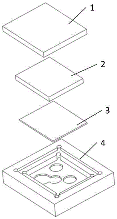
[0094] See figure 1 with figure 2 :

[0095] (1) Forming the base

[0096] Using high-purity graphite precision processing, four-layer cavities are milled by CNC machine tools. Cavity I is opened according to the distribution position of the dielectric bridge on the surface of the chip. Cavity II is used for chip placement and positioning. The cavity size is consistent with the chip eutectic position. The cavity height and chip thickness are 30μm lower. The size of the surface cavity is the same as that of the substrate, and the height is slightly lower than the thickness of the substrate by 30 μm.

[0097] (2) Substrate pretreatment

[0098] The substrate is a high thermal conductivity Mo80Cu20 alloy sheet, which is machined into the required 4mm×6mm×0.5mm, and the surface is plated with Au / Ni plating. The Au80Sn20 eutectic solder with a thickness of 12.7μm is preset on the surface to be bonded by the crimping method .

[0099] (3) Briquetting

[0100] The cover plate is an alumina...

Embodiment 2

[0107] See figure 1 with figure 2 :

[0108] (1) Forming the base

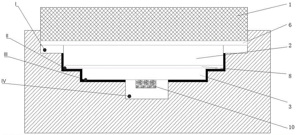
[0109] Using high-purity graphite precision processing, four-layer cavities are milled by CNC machine tools. Cavity I is opened according to the distribution position of the dielectric bridge on the surface of the chip. Cavity II is used for chip placement and positioning. The cavity size is consistent with the chip eutectic position. The cavity height and chip thickness are 30μm lower. The size of the surface cavity is the same as that of the substrate, and the height is slightly lower than the thickness of the substrate by 30μm. The specific structure is as follows image 3 Shown.

[0110] (2) Substrate pretreatment

[0111] The substrate is a high thermal conductivity W85Cu15 alloy sheet, which is machined into the required 10mm×6mm×2mm, and the surface is plated with Au / Ni plating. Pb37Sn63 eutectic solder with a thickness of 0.06mm is preset on the surface to be bonded by crimping.

[0112] (3) Briquetting

[01...


PUM


Abstract

The invention discloses a flip-chip eutectic bonding method for a chip with a medium bridge and an obtained product. The method comprises the following five steps: base molding; substrate pretreatment; pressing block molding; assembling; and eutectic bonding. The product comprises a cover board, a substrate, the chip and a base. The flip-chip eutectic bonding method has the beneficial technical effects that damage to the medium bridge on a bare chip graph layer in the assembly process is avoided; pollution and damage to a surface graph of the chip caused by a tray are avoided; high-precision positioning between the chip and the substrate is achieved; simultaneous eutectic bonding of a plurality of bare chips is achieved; overburning and solder oxidation in the eutectic bonding process of a multi-chip module are avoided; the reliability of a component is provided; the assembly efficiency is improved; the assembly failure rate is reduced; and batch assembly of a high-reliability and high-efficiency multi-chip module is achieved.

Description

technical field [0001] The invention belongs to the field of microelectronic packaging, and in particular relates to a chip flip-chip eutectic bonding method with a dielectric bridge and an obtained product. Background technique [0002] Chip assembly in microelectronics packaging technology is mainly realized by two mainstream processes such as conductive adhesive bonding and eutectic bonding. Compared with the former, eutectic bonding has the advantages of low resistivity, excellent thermal conductivity and low microwave loss. , is widely used in the assembly and packaging of high-power and microwave chips, and provides a highly reliable assembly method for military hybrid integrated circuits. [0003] Chip eutectic bonding is a way to realize the integration, miniaturization and light weight of microelectronic devices. In the application of microwave components, it has the characteristics of high application frequency, fast transmission rate and large bandwidth. Eutectic...

Claims


Application Information

Patent Timeline
Patent Type & Authority Applications(China)
IPC IPC(8): H01L21/60H01L21/50H01L23/31H01L23/488
CPCH01L21/50H01L23/31H01L23/488H01L24/02H01L24/03H01L24/26H01L24/31H01L24/80H01L24/83H01L2224/02H01L2224/03H01L2224/26H01L2224/31H01L2224/80
Inventor 闵志先邱颖霞胡骏林文海宋夏
Owner CHINA ELECTRONIC TECH GRP CORP NO 38 RES INST
Why Eureka
Try Eureka