High-reliability ultra-small metal ceramic surface-mounted device packaging process

A technology of metal ceramics and packaging technology, which is applied in the field of device packaging, can solve the problems of weak welding between chips and shells, not being widely used, and weak bonding of bonding wires, and achieves easy automation, easy integration, and low weight. light effect

Active Publication Date: 2016-03-23
济南市半导体元件实验所
View PDF5 Cites 8 Cited by
  • Summary
  • Abstract
  • Description
  • Claims
  • Application Information

AI Technical Summary

Problems solved by technology

However, due to the ultra-small cavity volume of ultra-small cermet surface mount devices, the chip soldering process and bonding process have always been the key process difficulties in the development of such devices in the packaging process, and the use of traditional packaging processes will generate heat. High resistance, weak welding of chip and shell, weak bonding of bonding wire, low reliability, etc., so it has not been widely used

Method used


Image

  • High-reliability ultra-small metal ceramic surface-mounted device packaging process
  • High-reliability ultra-small metal ceramic surface-mounted device packaging process
  • High-reliability ultra-small metal ceramic surface-mounted device packaging process

Examples


Embodiment Construction

[0032] The principles of the present invention are further described and explained below so that those skilled in the art can better understand the present invention. To be limited, all improvements within the idea of ​​the present invention should be within the protection scope of the present invention.

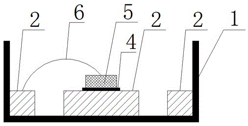
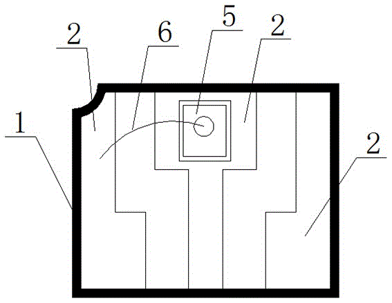
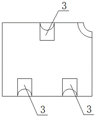
[0033] Such as Figure 1~3 As shown, it is a schematic diagram of a UB package device, Figure 4-6 Shown is a schematic diagram of a UA-type packaged device, the surface mount device includes a package 1, the tube core of the package 1 and two ends are provided with conductive areas 2, the chip 5 is welded on the conductive area 2 at the tube core, the chip 5 and The conductive area 2 at the end of the shell is electrically connected through the bonding wire 6 , and the back of the shell 1 is provided with a lead-out terminal 3 , which is electrically connected to the conductive area 2 . Compared with traditional devices, the highly reliable ultra-small cermet surface moun...


PUM

PropertyMeasurementUnit
thicknessaaaaaaaaaa
thicknessaaaaaaaaaa
diameteraaaaaaaaaa

Abstract

The invention discloses a high-reliability ultra-small metal ceramic surface-mounted device packaging process. The packaging process adopts a deep cavity gold-base soldering terminal eutectic soldering process and a deep cavity bonding process; a chip is welded on a tube shell by adopting the deep cavity gold-base soldering terminal eutectic soldering process; the welding is high in shearing force, low in thermal resistance and high in reliability, so that the thermal resistance and the saturation voltage drop of the device are reduced, and the thermal fatigue resistance of the device is improved; meanwhile, a chip welding process for various kinds of back surface materials can be satisfied; by adopting the small-sized deep cavity bonding process, the atomic-level contact of the bonding material is realized, and the reliability in the bonding wire welding of the device is improved; the automation of the process can be easily realized, and the production efficiency is improved; and the working range of the packaging process is from minus 65 DEG C to 200 DEG C. The packaged product can be widely applied to computers, radars, communication transmitters, aerospace crafts, instruments and the like.

Description

technical field [0001] The invention relates to a device packaging process, in particular to a highly reliable ultra-small cermet surface mount device packaging process, which belongs to the device packaging technology field. Background technique [0002] At present, a large number of easy-to-integrate surface mount devices are used in aerospace, aviation, ships, weapons and other fields, but they are all high-power and high-current devices. Small size, small thermal resistance, high efficiency, high reliability and other characteristics provide a prerequisite for improving the reliability of the whole machine and reducing the volume and weight of the whole machine system. However, due to the ultra-small inner cavity volume of ultra-small cermet surface mount devices, the chip welding process and bonding process have always been the key process difficulties in the development of such devices in the packaging process, and the use of traditional packaging processes will genera...

Claims


Application Information

Patent Timeline
Patent Type & Authority Applications(China)
IPC IPC(8): H01L21/60B23K37/00B23K101/36
CPCH01L2224/48091H01L2924/00014H01L24/01B23K37/00B23K2101/36H01L24/02H01L24/03H01L24/04H01L2224/01H01L2224/02H01L2224/03H01L2224/04
Inventor 赵志桓李东华张礼杜磊吕瑜
Owner 济南市半导体元件实验所
Why Eureka
Try Eureka