Modeling method for radio frequency MOS device and test structure

A technology for MOS devices and test structures, applied in the field of semiconductors, can solve the problems of limited flexibility, difficulties, and limitations of model correction methods, and achieve the effect of improving flexibility and improving accuracy

Active Publication Date: 2016-03-23
SHANGHAI INTEGRATED CIRCUIT RES & DEV CENT +1
View PDF5 Cites 20 Cited by
  • Summary
  • Abstract
  • Description
  • Claims
  • Application Information

AI Technical Summary

Problems solved by technology

This approach makes the design of the de-embedding auxiliary structure relatively simple, but it limits the flexibility of the back-channel interconnection layout under the de-embedding plane, and brings certain limitations to the optimal design of the circuit.
In addition, the device models of the intrinsic device part and the subsequent interconnection line part correspond to different working mechanisms, and have different changing laws as the device changes with the size, which requires selecting the same set of formulas to reflect the above two working mechanisms at the same time. It brings certain difficulties to establish a reasonable and accurate scalable (scalable) model, and also has certain limitations on the correction methods of the model

Method used


Image

  • Modeling method for radio frequency MOS device and test structure
  • Modeling method for radio frequency MOS device and test structure
  • Modeling method for radio frequency MOS device and test structure

Examples


Embodiment Construction

[0051] In order to make the content of the present invention clearer and easier to understand, the content of the present invention will be further described below in conjunction with the accompanying drawings. Of course, the present invention is not limited to this specific embodiment, and general replacements known to those skilled in the art are also covered within the protection scope of the present invention.

[0052] The following is attached Figure 1-11 The present invention will be described in further detail with specific examples. It should be noted that the drawings are all in a very simplified form, using imprecise scales, and are only used to facilitate and clearly achieve the purpose of assisting in describing the present embodiment.

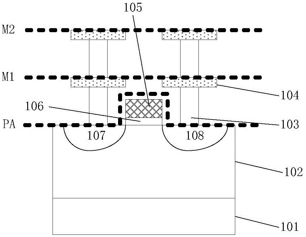
[0053] For this example, see figure 1 The MOS device test structure includes an intrinsic MOS device, a first interconnection layer located on the intrinsic MOS device, a first extraction pole and a first contact structure; the ...


PUM


Abstract

The invention provides a modeling method for a radio frequency MOS device and a test structure. Parasitic element values which cannot be removed by an existing de-embedding method are represented by virtue of an auxiliary test structure; the obtained original model of the test structure of the MOS device is corrected by these parasitic element values, so that parasitic factors caused by the test structure of the MOS device are completely removed; and planar propulsion of a de-embedding plane of the MOS device from a metal layer of a first interconnect metal layer to a polysilicon / active region (PA) plane is achieved to obtain a model of an intrinsic MOS device. According to the modeling method for the radio frequency MOS device and the test structure, an intrinsic model and a later parasitic model of the device can be respectively obtained by completely separating the parasitic factors except for the MOS device; building of a physically-based scalable MOS device model is facilitated aiming at the MOS devices with different sizes; the precision of the later model can be improved by a mature later interconnect modeling scheme in the industry; and limitations of the test structure are eliminated during device selection, so that the device selection and layout optimization flexibility is improved.

Description

technical field [0001] The invention relates to the technical field of semiconductors, in particular to a modeling method of a radio frequency MOS device and an auxiliary test structure applied to the modeling method. Background technique [0002] Accurate modeling of semiconductor devices plays a very important role in circuit design. The modeling process is mainly based on the test data of the characterization structure. Devices used in the radio frequency field are usually modeled by testing their scattering parameters (S parameters). The range of test frequencies must cover the operating frequency range of the device. In the test structure of the device, besides the intrinsic device to be tested, it is unavoidable to introduce a test contact block (pad) and an interconnection line between the pad and the device. In the application range of radio frequency or higher frequency, since the parasitic factors brought by the test pad of the device and the interconnection betwe...

Claims


Application Information

Patent Timeline
Patent Type & Authority Applications(China)
IPC IPC(8): H01L21/66G01R31/26G06F17/50
CPCG01R31/2639G01R31/2644G06F30/39H01L22/34
Inventor 刘林林郭奥周伟
Owner SHANGHAI INTEGRATED CIRCUIT RES & DEV CENT
Why Eureka
Try Eureka