Electronic static discharge (ESD) protection device with bidirectional silicon controlled rectifier (SCR) structure embedded with interdigital N-channel metal oxide semiconductor (NMOS)

A technology for ESD protection and devices, which is applied in the direction of electric solid-state devices, semiconductor devices, semiconductor/solid-state device parts, etc., can solve the problem of reducing the current density of the bidirectional SCR current conduction path, increasing the SCR conduction resistance, maintaining low voltage, etc. Problems, to achieve the effect of enhancing ESD robustness, increasing on-resistance, and maintaining voltage

Active Publication Date: 2016-03-23
JIANGNAN UNIV
View PDF5 Cites 23 Cited by
  • Summary
  • Abstract
  • Description
  • Claims
  • Application Information

AI Technical Summary

Problems solved by technology

[0004] Aiming at the ubiquitous problems of high trigger voltage, low maintenance voltage and insufficient latch-up resistance in existing ESD protection devices, an example of the present invention designs an ESD protection device with an embedded interdigitated NMOS bidirectional SCR structure, which is sufficient Utilizing the characteristics of the strong current discharge capability of SCR devices, the device forms an ESD current discharge path of PNPN structure under the action of ESD pulses, and through the resistance-capacitance coupling current path embedded with interdigitated NMOS and parasitic P-well resistance, it improves The response speed of the device reduces the current density in the bidirectional SCR current conduction path, increases the on-resistance of the SCR, and increases the maintenance voltage

Method used


Image

  • Electronic static discharge (ESD) protection device with bidirectional silicon controlled rectifier (SCR) structure embedded with interdigital N-channel metal oxide semiconductor (NMOS)
  • Electronic static discharge (ESD) protection device with bidirectional silicon controlled rectifier (SCR) structure embedded with interdigital N-channel metal oxide semiconductor (NMOS)
  • Electronic static discharge (ESD) protection device with bidirectional silicon controlled rectifier (SCR) structure embedded with interdigital N-channel metal oxide semiconductor (NMOS)

Examples


Embodiment Construction

[0025] Below in conjunction with accompanying drawing and specific embodiment the present invention will be described in further detail:

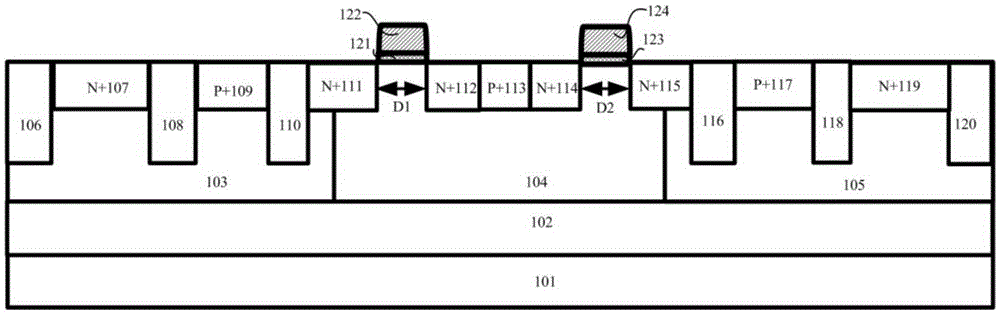
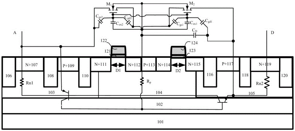
[0026] The example of the present invention designs an ESD protection device with an embedded interdigitated NMOS bidirectional SCR structure, which not only makes full use of the characteristics of the strong current handling capability of the SCR device, but also makes the device form an ESD current discharge path with a PNPN structure under the action of ESD pulses , and through the RC coupling current path embedded with interdigitated NMOS and parasitic P well resistance, the current density in the bidirectional SCR current conduction path is reduced, the on-resistance of the SCR is increased, and the sustaining voltage is increased.

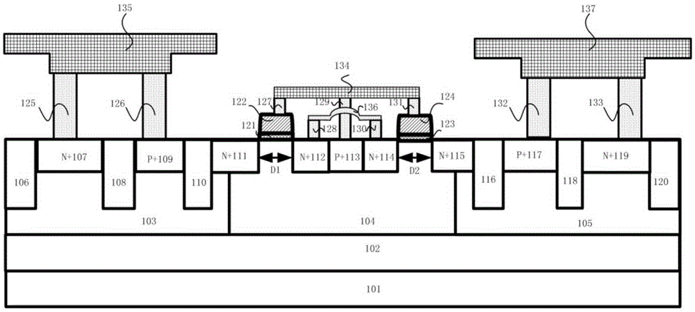
[0027] Such as figure 1 The shown cross-sectional view of the device structure of the example of the present invention is specifically an ESD protection device with an embedded interdigitated NMOS bidirec...


PUM


Abstract

An electronic static discharge (ESD) protection device with a bidirectional silicon controlled rectifier (SCR) structure embedded with an interdigital N-channel metal oxide semiconductor (NMOS) can be applied to an ESD protection circuit of an on-chip integrated circuit (IC) and mainly comprises a P substrate, a P epitaxial layer, a first N pit, a P pit, a second N pit, a first N+ injection region, a first P+ injection region, a second N+ injection region, a third N+ injection region, a second P+ injection region, a fourth N+ injection region, a fifth N+ injection region, a third P+ injection region, a sixth N+ injection region, a plurality of poly-silicon gates, a plurality of thin gate oxide layers and a plurality of shallow isolation grooves. On one hand, under the positive and negative ESD pulse effects, an ESD current discharge path with a symmetric structure and complete same electrical property exists in the device, the ESD current discharge ability of the device can be improved, and bidirectional protection of an ESD pulse is achieved; and on the other hand, the interdigital NMOS composed of an NMOS M<1> and an NMOS M<2> and a parasitic P pit resistor form a resistance-capacitance coupling current path, so that the ESD robustness of the device is enhanced, the current density in an SCR current conduction path is reduced, the conduction resistance of the SCR is increased, and the maintaining voltage is increased.

Description

technical field [0001] The invention belongs to the field of electrostatic discharge protection of integrated circuits, relates to a high-voltage ESD protection device, in particular to an ESD protection device with an embedded interdigitated NMOS bidirectional SCR structure, which can be used to improve the reliability of on-chip IC high-voltage ESD protection. Background technique [0002] The phenomenon of electrostatic discharge (ESD) is ubiquitous in nature. People's impression of electrostatic discharge is lightning or sparks when they take off their sweaters in winter. In the semiconductor industry, with the reduction of semiconductor size and the diversification of chip functions, the potential threat of electrostatic discharge to integrated circuits (IC) is becoming more and more obvious, and ESD protection design has become an important link in the reliability design of IC systems One, a good ESD protection design can enhance the circuit performance of the IC and p...

Claims


Application Information

Patent Timeline
Patent Type & Authority Applications(China)
IPC IPC(8): H01L27/02
CPCH01L27/0248H01L27/0262H01L27/0266H01L23/60H01L27/02
Inventor 梁海莲王鑫顾晓峰丁盛
Owner JIANGNAN UNIV
Why Eureka
Try Eureka