A kind of manufacturing method of partial thick copper pcb

A technology of local thick copper and manufacturing methods, which is applied in printed circuit manufacturing, reinforcement of conductive patterns, printed circuits, etc., can solve problems such as copper thickness limitation, complicated manufacturing process, inconsistent copper requirements on circuit board surface, etc., to improve product quality , The production process is simple, and the effect of avoiding the sandwich phenomenon

Active Publication Date: 2018-11-23
东莞森玛仕格里菲电路有限公司
View PDF4 Cites 0 Cited by
  • Summary
  • Abstract
  • Description
  • Claims
  • Application Information

AI Technical Summary

Problems solved by technology

[0002] The design and application of the existing circuit boards are becoming more and more specialized. Some circuit boards have inconsistent copper requirements on the circuit positions and copper layers, and some parts require thicker copper plating than other parts. However, the production process in the prior art is only It can control the copper thickness of the whole surface to be consistent, and it is difficult to meet the special surface copper requirements of local positions
At present, for the production of local thick copper PCBs, especially PCBs with a height difference exceeding 2 oz (ounces), due to the limited copper thickness in the local thick copper area, the manufacturing process is relatively complicated and difficult to manufacture.
The main production defects of this type of PCB are: 1. The method of making PCB with high and low copper thickness is long. In order to achieve a local copper thickness that is thicker than other places, it is necessary to repeat the processes of electroplating, film sticking, film removal, and etching many times, and the process is complicated. , prone to defects and scrapping, low yield rate
2. The height difference area is easy to cause the secondary film to be weak, which will affect the product quality

Method used


Image

  • A kind of manufacturing method of partial thick copper pcb
  • A kind of manufacturing method of partial thick copper pcb
  • A kind of manufacturing method of partial thick copper pcb

Examples


Embodiment Construction

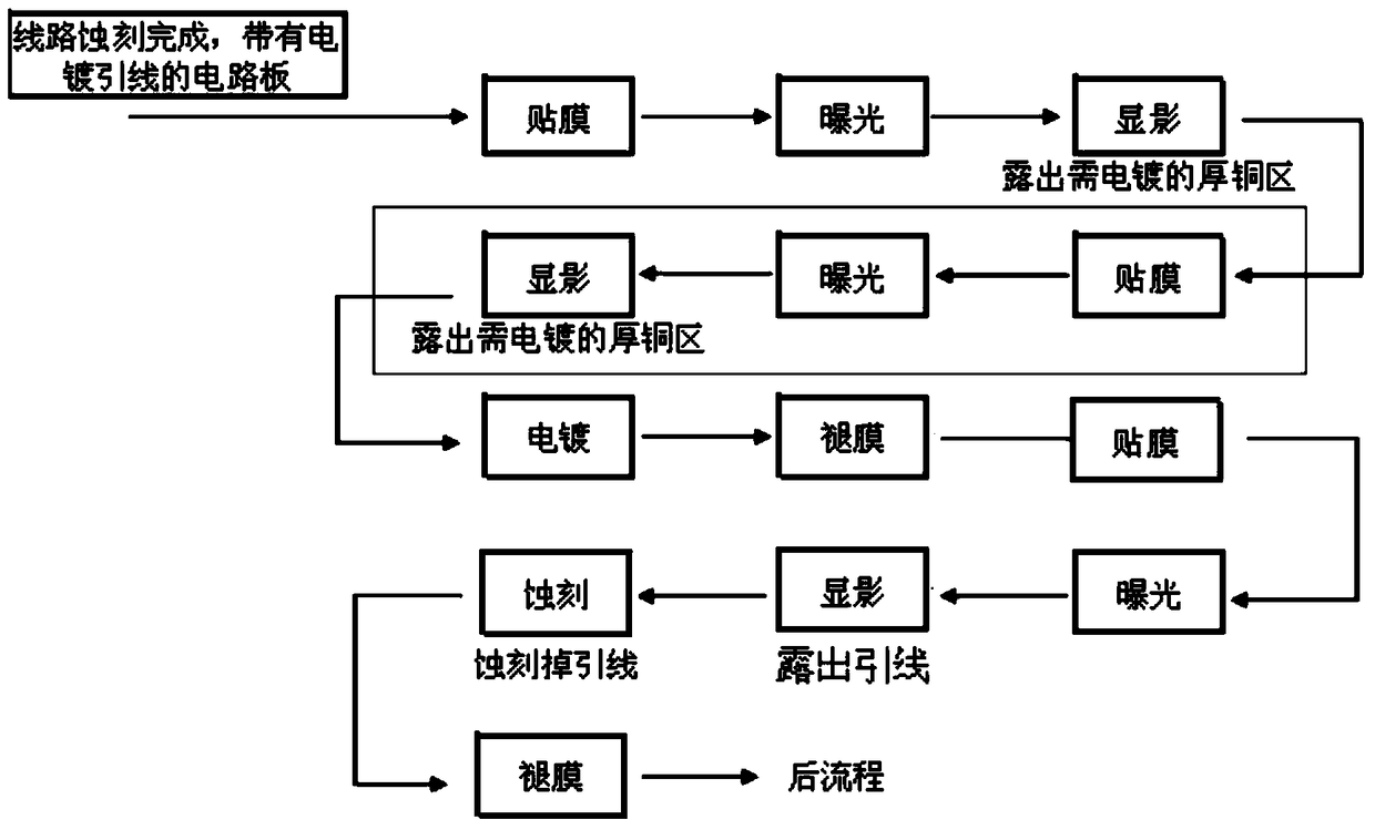
[0028] The present invention will be further described below in conjunction with the drawings and preferred embodiments, see Figure 1~8 As shown, a method for manufacturing a locally thick copper PCB includes the following steps:

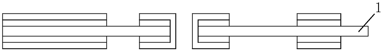
[0029] A. Preparation steps: etching the circuit board 1 to form a circuit board 1 with electroplated leads and partially thick copper to be made; the circuit board 1 is a double-sided or multilayer circuit board;

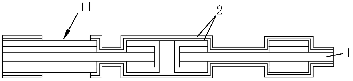
[0030] B. Pasting a dry film 2 step: Paste at least two layers of a dry film 2 on the area 11 of the circuit board 1 that does not require thick copper plating, and expose and develop the area 11 that requires thick copper plating; specifically:

[0031] B1. Paste the first layer of dry film 2 on the area 11 that does not require thick copper plating on the circuit board 1, and expose and develop the area 11 that requires thick copper plating;

[0032] B2. Paste an additional layer of the primary dry film 2 on the outer surface of the primary d...


PUM


Abstract

The present invention relates to the technical field of a PCB, and particularly relates to a manufacturing method of a locally thick copper PCB. The manufacturing method comprises the following steps: A, a step of preparation; B, a step of pasting primary dry films: pasting at least two layers of primary dry films in areas on a circuit board, where thick copper does not need to be plated, and carrying out exposure and development to expose areas where the thick copper needs to be plated; C, a step of locally plating the thick copper; D, a step of taking off the primary dry films; E, a step of pasting secondary dry films; F, a step of carrying out lead etching; and G, a step of taking of the secondary dry films. According to the manufacturing method disclosed by the present invention, a phenomenon of film clipping can be effectively avoided, and a local copper thickness can be made to be 2-3 oz and even greater according to the number of film pasting times, so that the difficult problem that the local copper thickness is greatly different from other areas to result in difficult production can be effectively solved; and moreover, the method is simple in manufacturing process, can well achieve local planting of the thick copper without special control, can be used for manufacturing products in batches, and cannot generate rejections basically, thereby enabling product yield to be very high and improving product quality.

Description

Technical field: [0001] The invention relates to the technical field of PCB boards, in particular to a method for manufacturing a locally thick copper PCB. Background technique: [0002] The design and application of existing circuit boards are becoming more and more specialized. Some circuit boards have inconsistent copper requirements for the circuit position table, and some areas require thicker copper plating than others. However, the production process in the prior art is only The copper thickness of the whole surface can be controlled to be consistent, and it is difficult to meet the requirements of special surface copper in local locations. At present, for the production of locally thick copper PCBs, especially PCBs with a height difference of more than 2oz (ounces), due to the limited copper thickness in the local thick copper areas, the production process is relatively complicated and the production difficult. The main production defects of this type of PCB are: 1. The ...

Claims


Application Information

Patent Timeline
Patent Type & Authority Patents(China)
IPC IPC(8): H05K3/24
CPCH05K3/243H05K2201/098
Inventor 冯启民周勇胜
Owner 东莞森玛仕格里菲电路有限公司
Why Eureka
Try Eureka