FinFET and preparation method thereof

A technology of fins and substrates, which is applied in semiconductor/solid-state device manufacturing, electrical components, circuits, etc., can solve the problems of doping dose loss and affecting SSRW morphology, etc., to reduce device power consumption and improve carrier migration rate, to achieve the effect of the isolation effect

Active Publication Date: 2016-03-30
SEMICON MFG INT (SHANGHAI) CORP
View PDF4 Cites 10 Cited by
  • Summary
  • Abstract
  • Description
  • Claims
  • Application Information

AI Technical Summary

Problems solved by technology

At present, a SSRW (SuperSteep Retrograde Well) technology has been developed to effectively improve carrier mobility, but this technology has only been widely used in planar FETs, but it is still difficult to perfect the SSRW technology. Application to the preparation of FinFET
This is because in the FinFET, if the width of the raised fin structure (Fin) is too small, the ions implanted into the FinFET are easily diffused into the shallow trench dur

Method used


Image

  • FinFET and preparation method thereof
  • FinFET and preparation method thereof
  • FinFET and preparation method thereof

Examples


preparation example Construction

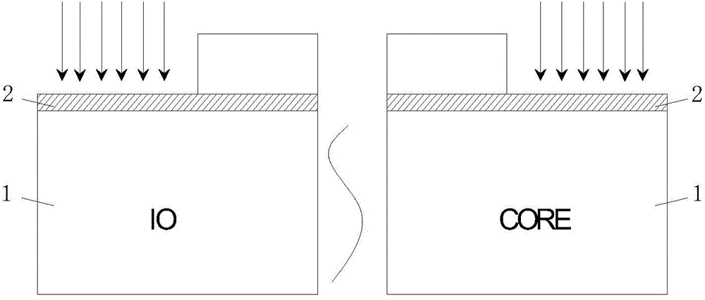
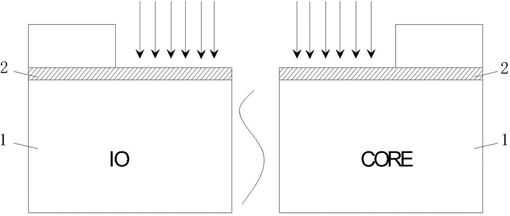
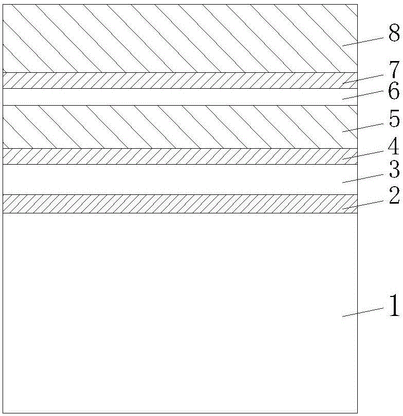
[0042] The present invention provides a FinFET preparation method. In the present invention, SSRW technology can be well applied to three-dimensional FinFET preparation. Refer to Figure 1-20 As shown, the specific steps are as follows,

[0043] Step S1: First, a semiconductor substrate 1 is provided, and a pad oxide layer 2 (PAD oxide) is prepared on the upper surface of the substrate. This substrate 1 includes IO (InputOutput, input and output) device area and core (CORE) device area, and IO device area and core device area all define NMOS area and PMOS area; The PMOS area is subjected to one or more ion implantation processes, specifically: using a photolithography process, using photoresist to block the IO device area and the PMOS area in the core device area, and then using the photoresist as a mask to cover the NMOS area. Ion implantation is performed in the region; after that, the same steps are performed, and the NMOS region is blocked by photoresist, and ion implantat...


PUM


Abstract

The invention provides an FinFET and a preparation method thereof. Trenches among adjacent fin-shaped structures form shallow trench isolation structures (STI), and oxide layers and insulation material layers are arranged among shallow trenches, the fin-shaped structures and a substrate, so that isolation effect can be achieved well, and diffusion of doping-ions in the fin-shaped structures and the substrate can be avoided; iron injection of high dose C-co or high dose F-co in the conventional FinFET preparation process can be avoided, so that the damage to the substrate and the fin-shaped structures due to the bombardment effect during iron injection can be reduced; and furthermore, the form of an SSRW also can be maintained well, the carrier mobility can be effectively improved, and the performance of the device can be greatly improved.

Description

technical field [0001] The invention relates to a method for preparing a semiconductor, to be precise, relates to a FinFET and a method for preparing the same. Background technique [0002] Field Effect Transistor (FieldEffect Transistor, FET) is conducted by majority carriers, also known as unipolar transistor. It is a voltage-controlled semiconductor device. It has the advantages of high input resistance, low noise, low power consumption, large dynamic range, easy integration, no secondary breakdown phenomenon, and wide safe working area, and is widely used in the field of semiconductor preparation. With the continuous maturity of FET technology and people's continuous pursuit of high-performance devices, Professor Hu Zhengming of the University of California, Berkeley developed a new type of field effect transistor—FinFET (Fin Field Effect Transistor). In the structure of FinFET, the gate Formed into a fork-shaped 3D structure similar to a fish fin, it can control the o...

Claims


Application Information

Patent Timeline
IPC IPC(8): H01L29/78H01L29/06H01L21/336
Inventor 李勇
Owner SEMICON MFG INT (SHANGHAI) CORP
Why Eureka
Try Eureka