Control method for enhancing organic solderability preservative (OSP) tin soldering property

A control method and process technology, applied in the field of OSP, can solve problems such as poor tin on PCB boards, and achieve the effect of maintaining tinning and good tinning.

Inactive Publication Date: 2016-03-30
HUIZHOU ZHONGJING ELECTRONICS TECH CO LTD
View PDF3 Cites 8 Cited by
  • Summary
  • Abstract
  • Description
  • Claims
  • Application Information

AI Technical Summary

Problems solved by technology

[0005] The purpose of the present invention is to provide a method for controlling tinning on OSP. The technical solution provided by the invention solves the technica...

Method used


Image

  • Control method for enhancing organic solderability preservative (OSP) tin soldering property

Examples


Embodiment

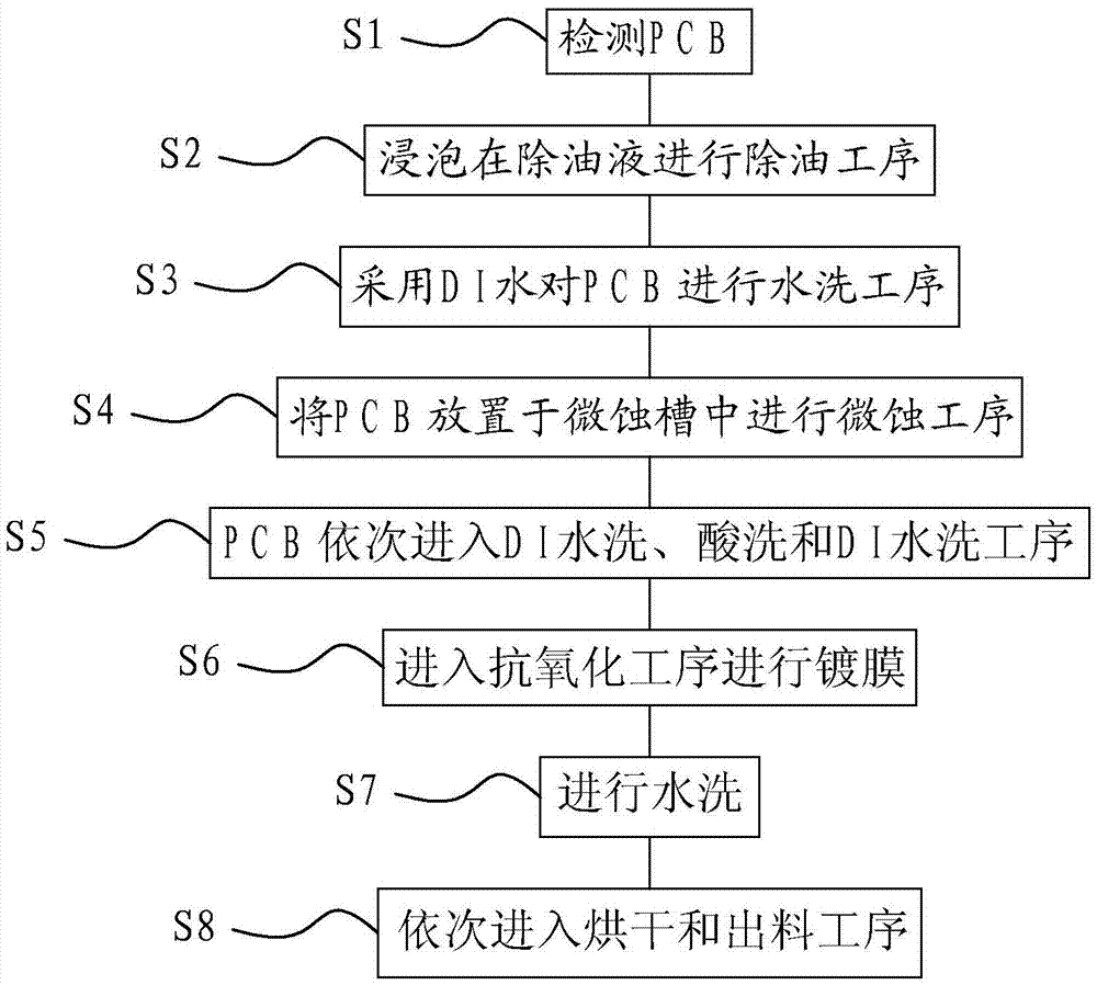
[0024] Such as figure 1 As shown, this embodiment discloses a control method for improving the tinning property of OSP, and the OSP process includes the following steps:

[0025] S1. Detect PCB

[0026] In this process, the good-quality PCB after the test is transferred to the final visual inspection to confirm the cleanliness of the PCB surface. At the same time, 10-20sets are taken from each batch for copper chloride test, and the cleanliness of the PCB surface does not meet the requirements. When the process is improved on the PCB, when the cleanliness of the PCB board surface meets the requirements, the PCB enters the degreasing process.

[0027] S2. Soak in degreasing liquid for degreasing process

[0028] The PCB with qualified cleanliness is soaked in a degreasing solution to perform a degreasing process, and the degreasing effect directly affects the film-forming quality. If the oil removal is not good, the thickness of the film will be uneven. On the one hand, the...


PUM

PropertyMeasurementUnit
Conductivityaaaaaaaaaa

Abstract

The invention relates to the technical field of organic solderability preservatives (OSPs), in particular to a control method for enhancing an organic solderability preservative (OSP) tin soldering property. According to the technical scheme provided by the invention, a printed circuit board (PCB) is detected firstly in order to ensure the cleanliness of a copper surface before coating of an OSP film. A film is formed under a good OSP condition, and the formed film is protected in inspection, conveying and packaging processes. Conditions which tend to occur before, during and after an OSP procedure are controlled to prevent hidden troubles, so that the technical problem of poor tin soldering property of the PCB due to poor OSP film control is solved, and good tin soldering property of the PCB treated with the OSP is kept.

Description

technical field [0001] The invention relates to the technical field of OSP, in particular to a control method for improving the tinning property of OSP. Background technique [0002] OSP is a process that meets the requirements of the RoHS directive for the surface treatment of printed circuit board (PCB) copper foil. It is translated as organic solder protection film, also known as copper protection agent. Simply put, OSP is to chemically grow an organic film on a clean bare copper surface. [0003] This layer of organic film has anti-oxidation, thermal shock resistance, and moisture resistance, and is used to protect the copper surface from rusting (oxidation or vulcanization, etc.) in a normal environment; but in the subsequent welding high temperature, this protective film must be It is easy to be quickly removed by flux, so that the exposed clean copper surface can be cleanly combined with molten solder in a very short time to form a firm solder joint. Due to the char...

Claims


Application Information

Patent Timeline
IPC IPC(8): H05K3/28
CPCH05K3/282H05K2203/0392
Inventor 戴晨曦李小王刘德林
Owner HUIZHOU ZHONGJING ELECTRONICS TECH CO LTD
Why Eureka
Try Eureka