Thin film-packaged OLED screen body and preparation method thereof

A thin-film encapsulation and electrode layer technology, which is used in semiconductor/solid-state device manufacturing, electrical solid-state devices, semiconductor devices, etc.

Active Publication Date: 2016-04-06
GUAN YEOLIGHT TECH CO LTD
View PDF3 Cites 12 Cited by
  • Summary
  • Abstract
  • Description
  • Claims
  • Application Information

AI Technical Summary

Problems solved by technology

[0005] The technical problem to be solved by the present invention is that the existing passive electroluminescent device (PMOLED) adopts thin-film packaging, which is prone to damage and leads to lax packaging, so as to provide a thin-film-encapsulated OLED screen body. The thin-film-encapsulated OLED screen By providing a planarization layer with a continuous planar structure, the thin film encapsulation layer can be closely attached to it, thereby preventing the damage of the thin film encapsulation layer

Method used


Image

  • Thin film-packaged OLED screen body and preparation method thereof
  • Thin film-packaged OLED screen body and preparation method thereof

Examples


Embodiment 1

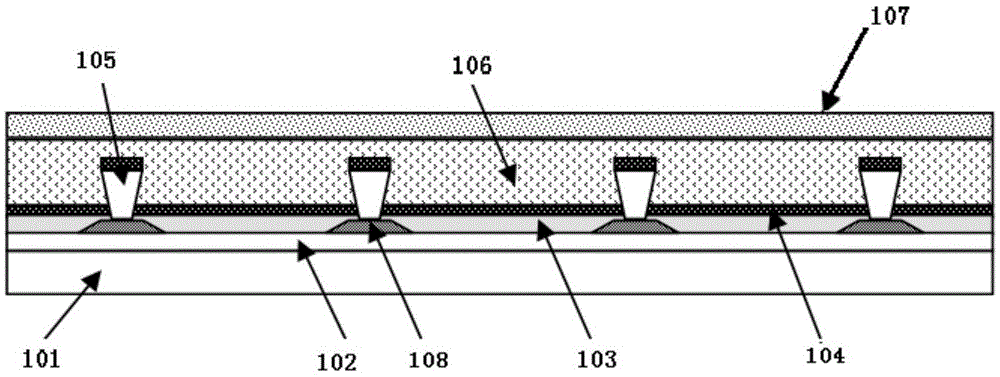
[0047] Such as figure 1 As shown, the thin-film-encapsulated OLED screen body of this embodiment includes a substrate 101 and a first electrode layer 102 (anode) disposed on the substrate 101, and several electrodes forming a continuous grid are arranged on the first electrode layer 102. The pixel definition layer 108 of the structure, the organic functional layer 103 is filled in the grid structure, the isolation column 105 is arranged above the pixel definition layer 108, and the second electrode on the adjacent organic function layer 103 is connected by the isolation column 105 Layers 104 (the cathodes) are insulated from each other. The shown organic functional layer 103 includes a stacked hole injection layer, a hole transport layer, a light emitting layer, an electron transport layer and an electron injection layer, wherein the hole injection layer, the hole transport layer, the electron transport layer and the electron injection layer One or more layers may be omitted....

Embodiment 2

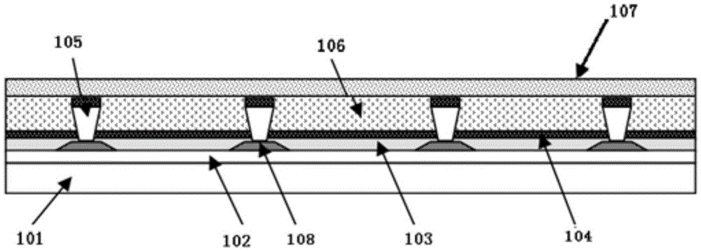
[0056] Such as figure 2 As shown, the structure of the film-encapsulated OLED screen of this embodiment is the same as that of Embodiment 1, wherein the planarization layer 106 is filled between the spacers 105, and its upper end and the top of the spacer 105 jointly form a continuous planar structure. The thin film encapsulation layer 107 is attached and disposed on the continuous planar structure.

[0057] Its preparation method is the same as that of the film-encapsulated OLED screen of Example 1, wherein step S3 is:

[0058] A planarization layer 106 is formed by evaporating an inorganic material above the second electrode layer 104, and the planarization layer 106 is filled between the isolation columns, and its upper end and the upper end of the isolation columns jointly form a continuous planar structure; or by printing The planarization layer 106 made of organic material is prepared by means of , silk printing, thermal deposition, etc., and its upper end and the uppe...

Embodiment 3

[0062] Such as figure 1 As shown, the structure of the thin-film-encapsulated OLED panel of this embodiment is the same as that of Embodiment 1, wherein the planarization layer 106 and the thin-film encapsulation layer 107 are an integrated structure made of polyhydrogensilazane materials. The molecular formula of silazane materials such as [SiH 2 NH], this type of material is prepared on the second electrode layer by wet coating or screen printing, and the polyhydrogensilazane type material reacts with moisture and oxygen in the air to form a cured film to form an integrated structure planarization layer 106 . After that, SiN or SiO is deposited by CVD as the thin film encapsulation layer 107 .

[0063] The mechanism of the reaction of silazane with water and oxygen is as follows, and the final buffer material is a silicon dioxide layer.

[0064] -[SiH 2 NH] n -+O 2 → SiO 2 +NH 3

[0065] and

[0066] -[SiH 2 NH] n -+H 2 O→SiO 2 +NH 3 +H 2

[0067] The prepar...


PUM

PropertyMeasurementUnit
transmittivityaaaaaaaaaa
refractive indexaaaaaaaaaa

Abstract

The invention relates to a thin film-packaged OLED screen body and a preparation method thereof. The thin film-packaged OLED screen body comprises a conductive substrate and a thin film package layer, wherein an organic functional layer is arranged in an airtight space formed by the conductive substrate and the thin film package layer; second electrode layers are arranged at the upper part of the organic functional layer; the adjacent second electrode layers are insulated with each other; a flatten layer is arranged between the thin film package layer and the second electrode layer; a continuous plane structure is formed at one side, far away from the second electrode layers, of the flatten layer; and the thin film package layer is attached to the continuous plane structure. The thin film package layer is formed at one side, opposite to a continuous plane, of the flatten layer, so that the thin film package layer can be tightly attached to the flatten layer; the thickness uniformity is good; the packaging effect is good; and the thin film package layer cannot be easily damaged.

Description

technical field [0001] The invention relates to the technical field of organic electroluminescent devices, in particular to a film-encapsulated OLED screen body and a preparation method thereof. Background technique [0002] After nearly 30 years of development, thin-film-encapsulated OLED screen (English full name OrganicLightEmittingDevice, referred to as OLED) as the next generation of lighting and display technology, has a wide color gamut, fast response, wide viewing angle, no pollution, high contrast, flat screen It has been applied to a certain extent in lighting and display. A typical film-encapsulated OLED screen generally includes a transparent substrate, a transparent anode, a reflective electrode, and an organic functional layer disposed between the two electrodes. Usually the cathode of the bottom-emitting OLED is a flat metal, which has a good reflection effect. [0003] The thin-film encapsulated OLED screen (OLED) includes active electroluminescent devices ...

Claims


Application Information

Patent Timeline
Patent Type & Authority Applications(China)
IPC IPC(8): H01L27/32H01L51/52H01L51/56
CPCH10K59/17H10K50/8428H10K71/00
Inventor 张国辉王静赵杨陈旭
Owner GUAN YEOLIGHT TECH CO LTD
Why Eureka
Try Eureka