Nanosilicon thin-film multi-junction solar cell

A technology for solar cells and nano-silicon thin films, applied in the field of solar cells, can solve the problems of low open-circuit voltage and filling factor, large light-induced attenuation, and low conversion efficiency of nano-silicon solar cells, so as to avoid interface effects and reduce light-induced degradation. effect, the effect of improving the photoelectric conversion efficiency

Inactive Publication Date: 2016-04-06
上海正相实业有限公司
View PDF5 Cites 2 Cited by
  • Summary
  • Abstract
  • Description
  • Claims
  • Application Information

AI Technical Summary

Problems solved by technology

[0011] The purpose of the present invention is to solve the problems of low conversion efficiency, large light-induced attenuation and low open-circuit voltage and fill factor of nano-silicon solar cells in traditional silicon thin-film solar cells, and provides a nano-silicon thin-film multi-junction solar cell to improve existing cells The structure and preparation process overcome the shortcomings and deficiencies in the prior art to achieve the improvement of battery efficiency

Method used


Image

  • Nanosilicon thin-film multi-junction solar cell

Examples


Embodiment Construction

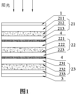
[0022] see figure 1 , the nano-silicon thin film double-junction solar cell of the present invention comprises a positive electrode layer 1 and a negative electrode layer 3, and three P-I-N junctions (subcells) 21, 22 and 23 are arranged between the positive electrode layer 1 and the negative electrode layer 3 as photoelectric In the conversion layer, the P-I-N junction 21 is the top cell, and the P-I-N junction 23 is the bottom cell. The P-I-N junction 21 is composed of a P-type silicon film layer 211, an intrinsic silicon film absorbing layer 212 and an N-type silicon film layer 213, and the P-I-N junction 22 is composed of a P-type silicon film layer 221, an intrinsic silicon film absorbing layer 222 and an N-type silicon film layer. The silicon thin film layer 223 is stacked in sequence, and the P-I-N junction 23 is composed of a P-type silicon thin film layer 231, an intrinsic silicon thin film absorption layer 232 and an N-type silicon thin film layer 233. Coupling laye...


PUM


Abstract

The invention discloses a nanosilicon thin-film multi-junction solar cell which comprises a positive electrode layer and a negative electrode layer. A plurality of P-I-N junctions are arranged between an anode layer and a cathode layer as a photoelectric conversion layer. Each P-I-N junction is obtained through successively laminating a P-type silicon thin-film layer, an intrinsic silicon film absorbing layer and an N-type silicon thin-film layer. A coupling connecting layer is arranged between two adjacent P-I-N junctions. In a direction from a top cell to a bottom cell, the thickness and the refractive index of the intrinsic silicon film absorbing layer gradually increase according to a geometric gradient, thereby introducing photons to advance, reducing surface reflection loss, successively reducing band gap widths gradually, improving absorption to a solar spectrum, reducing light-induced degradation, and realizing effective conversion efficiency improvement of the solar cell.

Description

technical field [0001] The invention relates to a solar cell technology, in particular to a multi-junction solar cell with a nano-silicon thin film. Background technique [0002] The optical bandgap width of amorphous silicon is 1.7eV, which makes the material itself insensitive to the long-wavelength region of the solar radiation spectrum, which limits the conversion efficiency of amorphous silicon solar cells. In addition, its photoelectric efficiency will decay with the continuation of the illumination time, which is the so-called light-induced degradation S-W effect, making the battery performance unstable. [0003] Existing nano-silicon thin-film solar cells cannot fully absorb solar light energy in different bands, have low power conversion efficiency, large light-induced attenuation, and low open-circuit voltage and fill factor of nano-silicon solar cells. [0004] Amorphous silicon thin-film multi-junction solar cells are considered to be a stable, high-efficiency, ...

Claims


Application Information

Patent Timeline
Patent Type & Authority Applications(China)
IPC IPC(8): H01L31/076H01L31/046H01L31/077
CPCY02E10/547Y02E10/548
Inventor 宋太伟高伟波方祥杨光余文凤张长华
Owner 上海正相实业有限公司
Why Eureka
Try Eureka