Supercharge Your Innovation With Domain-Expert AI Agents!

Array substrate, radiation detector, and wiring substrate

A technology of array substrates and substrates, which is applied in the fields of array substrates, radiation detectors and wiring substrates, and can solve problems such as cost increase and equipment size expansion

Active Publication Date: 2016-04-06
CANON ELECTRON TUBES & DEVICES CO LTD
View PDF5 Cites 3 Cited by
  • Summary
  • Abstract
  • Description
  • Claims
  • Application Information

AI Technical Summary

Problems solved by technology

However, this entails an increase in equipment size and cost

Method used


Image

  • Array substrate, radiation detector, and wiring substrate
  • Array substrate, radiation detector, and wiring substrate
  • Array substrate, radiation detector, and wiring substrate

Examples


Embodiment Construction

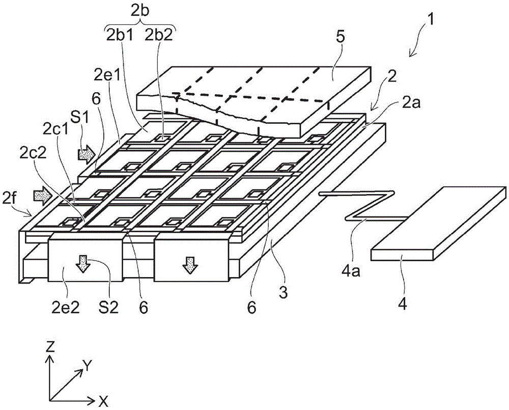
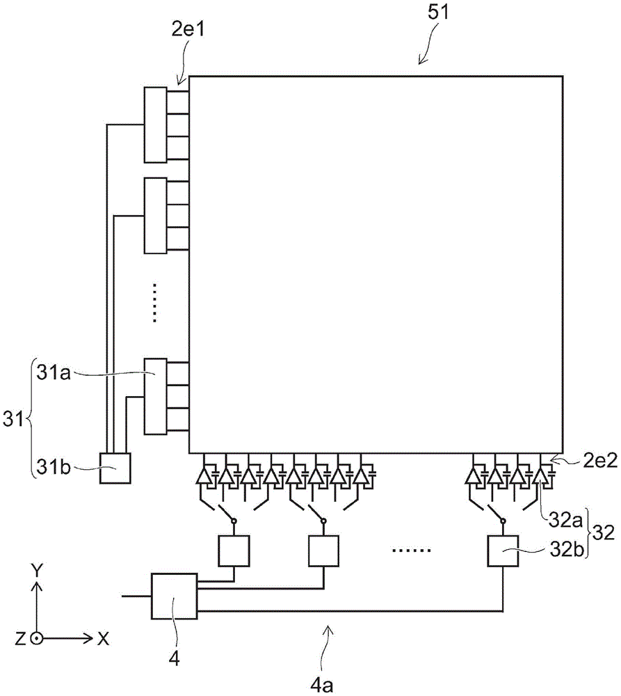
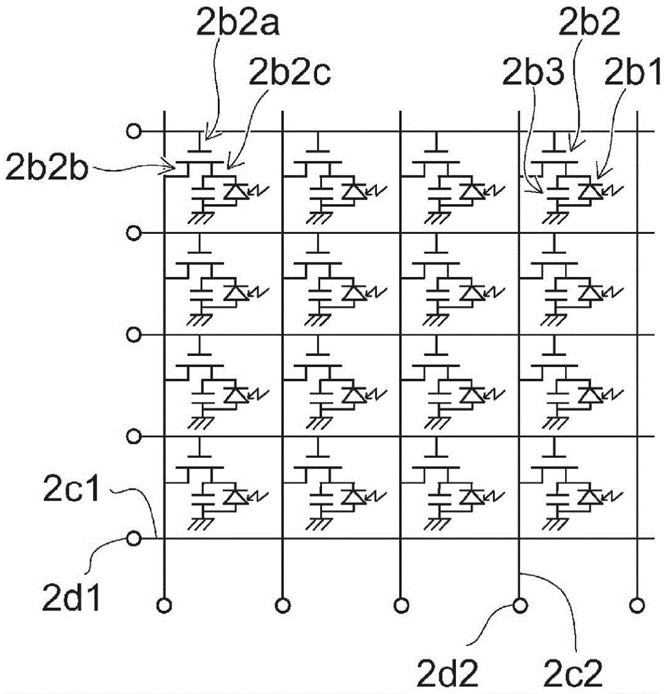
[0029] Hereinafter, various embodiments will be described with reference to the accompanying drawings. In the respective drawings, the same components are denoted by like reference numerals, and their detailed descriptions are omitted as appropriate.

[0030] The wiring substrate according to the embodiment of the present invention may be, for example, a plate-shaped substrate including a wiring pattern thereon. Circuit elements such as semiconductor elements are electrically connected to the wiring patterns.

[0031] An array substrate is an example of such a wiring substrate. The array substrate may be, for example, a plate-like substrate on which wiring patterns are included. Circuit elements such as thin film transistors and photodiodes are electrically connected to the wiring patterns. Such array substrates are used, for example, in flat panel displays and radiation detectors.

[0032] As an example, the present embodiment is described with reference to a radiation de...


PUM


Abstract

An array substrate according to an embodiment comprises: a substrate; a plurality of first wiring lines that are provided on a surface of the substrate and that extend in a first direction; a plurality of second wiring lines that are provided on the surface of the substrate and that extend in a second direction intersecting the first direction; thin-film transistors provided in respective regions defined by the plurality of first wiring lines and the plurality of second wiring lines; a protection layer that covers at least the plurality of first wiring lines and the plurality of second wiring lines; and a plurality of connection parts that are provided on the protection layer and / or between the plurality of first wiring lines and the substrate and / or between the plurality of second wiring lines and the substrate, the connection parts being electrically connected to the respective first wiring lines and the respective second wiring lines and including an electroconductive material that has a higher corrosion resistance than the material(s) of the first wiring lines and the second wiring lines. An end surface of each first wiring line and second wiring line on the peripheral edge side of the substrate is covered by the protection layer, and an end surface of each connection part on the peripheral edge side of the substrate is provided at the position of the peripheral edge of the substrate in a planar view.

Description

technical field [0001] Embodiments of the present invention relate to an array substrate, a radiation detector, and a wiring substrate. Background technique [0002] The wiring substrate may be provided with some circuit elements that are less resistant to static electricity. For example, semiconductor elements such as TFT (Thin Film Transistor) and MOSFET (Metal Oxide Semiconductor Field Effect Transistor), and photoelectric conversion elements such as photodiodes are generally low in resistance to static electricity. Therefore, manufacturing a wiring substrate provided with, for example, circuit elements less resistant to static electricity requires dissipating static electricity generated during the manufacturing process. For example, an outer short ring is provided around a region where circuit elements are provided so that static electricity generated during a manufacturing process is discharged through the outer short ring. [0003] An array substrate is an example o...

Claims


Application Information

Patent Timeline
IPC IPC(8): H01L27/146G01T1/20G01T7/00H01L21/3205H01L21/768H01L21/822H01L23/522H01L27/04H01L27/144H01L29/786H01L31/10H04N5/32
CPCH01L27/124H01L27/14603H01L27/14612H01L27/14636H01L27/14663H01L27/1446
Inventor 泷川达也榛叶勇一
Owner CANON ELECTRON TUBES & DEVICES CO LTD
Features
  • R&D
  • Intellectual Property
  • Life Sciences
  • Materials
  • Tech Scout
  • Unparalleled Data Quality
  • Higher Quality Content
  • 60% Fewer Hallucinations
Learn More