Planar annular microstrip slow-wave structure

A slow-wave structure, ring-type technology, applied to the circuit components of transit-time electron tubes, etc., can solve problems such as narrow frequency band, and achieve the effect of wide operating bandwidth, high coupling impedance, and small gain fluctuation.

Inactive Publication Date: 2016-04-13
UNIV OF ELECTRONICS SCI & TECH OF CHINA
View PDF10 Cites 16 Cited by
  • Summary
  • Abstract
  • Description
  • Claims
  • Application Information

AI Technical Summary

Problems solved by technology

[0007] On the basis of the three-dimensional ring-rod structure, the present invention proposes a two-dimensional planar ring microstrip slow-wave structure, which has a wider working bandwidth and higher coupling impedance, effectively solving the three-dimensional ring-rod structure. The problem of the narrow frequency band of the rod slow wave structure; compared with the existing microstrip slow wave structure, under the same size, the planar ring-rod microstrip slow wave structure can work in a higher frequency band, which requires electron guns and focusing magnetic fields is also relatively low, so it is a slow wave structure suitable for miniaturized planar traveling wave tubes with great potential

Method used


Image

  • Planar annular microstrip slow-wave structure
  • Planar annular microstrip slow-wave structure
  • Planar annular microstrip slow-wave structure

Examples


Embodiment

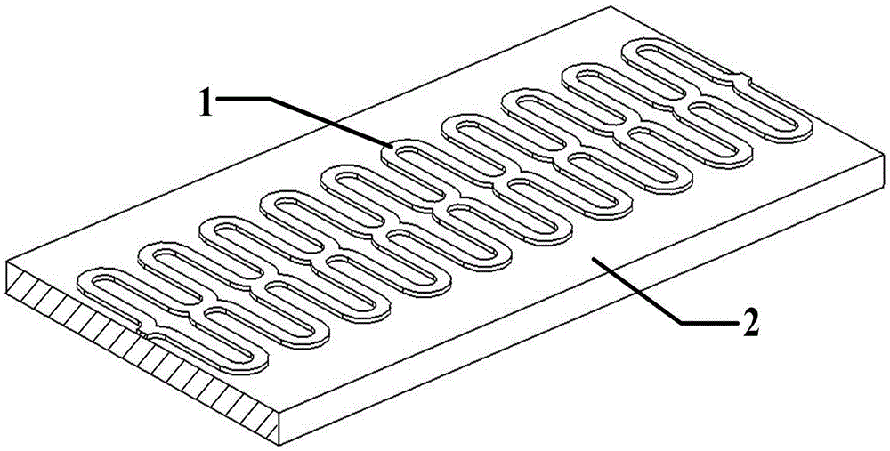
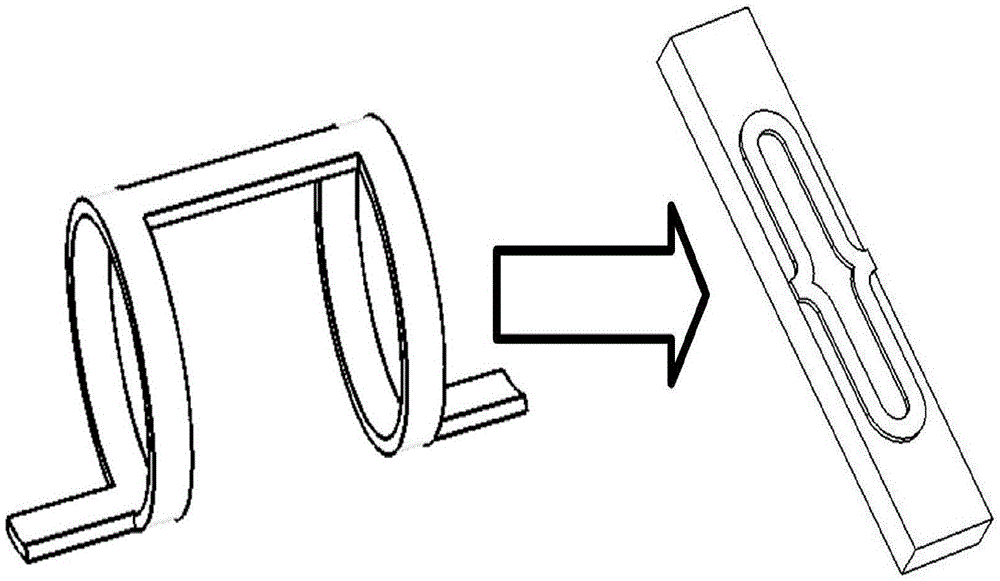
[0027] A planar annular slow-wave structure, such as figure 1 As shown, this figure is a structural schematic diagram of a specific embodiment of the present invention, including a dielectric substrate 2 and a metal wire 1 located on the surface of the dielectric substrate 2, and the metal wire 1 is sequentially connected by a plurality of ring units with the same shape and size A periodic structure is formed, each ring unit is formed by butting two split rings with upper and lower mirror mirrors, and two adjacent ring units are connected by a microstrip line at the junction of the two split rings.

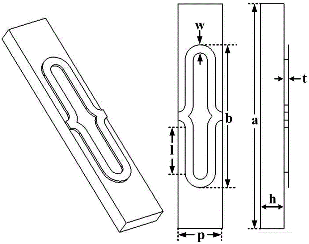
[0028] Such as figure 2 As shown, the dimension of the above-mentioned planar annular microstrip slow-wave structure is defined as follows: the dielectric constant of the dielectric substrate 2 is ε, the thickness of the dielectric substrate is h, the line width of the metal wire 1 is w, and the thickness is t, and the metal microstrip The transverse length of the belt loop is b...


PUM


Abstract

The invention discloses a planar annular microstrip slow-wave structure which belongs to the field of microwave electric vacuum technology. The planar annular microstrip slow-wave structure relates to a traveling-wave tube amplifier device. The planar annular microstrip slow-wave structure comprises a dielectric substrate (2) and metal wires (1) on the surface of the dielectric substrate (2). The planar annular microstrip slow-wave structure is characterized in that each metal wire (1) has a periodical structure which is obtained through successively connecting a plurality of annular units with same shape and same dimension. Each annular unit is obtained through joining two open rings which are in mirror symmetry in a vertical direction. Two adjacent annular units are connected at a joining part between the two open rings through a microstrip line. Compared with an existing microstrip slow-wave structure, the planar annular microstrip is advantageous in that a vacuum device with the planar annular microstrip slow-wave structure can be used in a higher operating frequency band on condition of same dimension because of wider cold bandwidth. The planar annular microstrip slow-wave structure provided by the invention has a wide transverse dimension, thereby effectively reducing a requirement for an electronic gun and a focusing magnetic field. The planar annular microstrip slow-wave structure has a relatively high coupling impedance and can perform interaction with an electron beam in a relatively good manner. Therefore the planar annular microstrip slow-wave structure has relatively high potential and is suitable for miniature planar traveling-wave tubes.

Description

technical field [0001] The design of the invention belongs to the field of microwave electric vacuum technology, and relates to a traveling wave tube amplifier. Background technique [0002] Traveling wave tube amplifier is a microwave vacuum device that amplifies high-frequency signals through the energy exchange between electromagnetic field and electron beam. As an important microwave power source, traveling wave tube plays a pivotal role in the field of vacuum electronics due to its advantages of high power, high gain, high efficiency, broadband and long life, and is widely used in electronic countermeasures, communications, field of guidance. [0003] At present, helical traveling wave tubes and coupled cavity traveling wave tubes are the most widely used in various fields. The helical slow wave structure is a slow wave system widely used in traveling wave tubes. The helical slow-wave structure has the advantage of wide operating bandwidth, but it is bulky and very bu...

Claims


Application Information

Patent Timeline
Patent Type & Authority Applications(China)
IPC IPC(8): H01J23/24
CPCH01J23/24H01J2223/24
Inventor 丁冲魏彦玉李倩张鲁奇王媛媛赵国庆王文祥宫玉彬
Owner UNIV OF ELECTRONICS SCI & TECH OF CHINA
Why Eureka
Try Eureka