On-chip array thermoelectric converter of field effect transistor and fully-automatic alignment manufacturing technology thereof

A field effect transistor and manufacturing process technology, which is applied to the field effect transistor on-chip array thermoelectric converter and its fully self-aligned manufacturing process field, can solve the problems of insufficient overload capacity, poor dynamic characteristics, slow response speed, etc., and achieves dynamic characteristics and Excellent overload characteristics, fast response speed, and the effect of measuring frequency bandwidth

Inactive Publication Date: 2014-08-13
GANNAN NORMAL UNIV
View PDF4 Cites 4 Cited by
  • Summary
  • Abstract
  • Description
  • Claims
  • Application Information

AI Technical Summary

Problems solved by technology

[0005] In order to overcome the shortcomings of the existing thermoelectric conversion mode, such as narrow frequency band, slow response speed, poor dynamic characteristics, insufficient overload capacity, complicated processing technology and high cost, the technical problem to be solved by the present invention is to provide a wide frequency band, fast response speed As well as better dynamic characteristics and overload characteristics, novel structure, simple processing technology, and low cost field effect tube-on-chip array thermoelectric converter and its fully self-aligned manufacturing process

Method used


Image

  • On-chip array thermoelectric converter of field effect transistor and fully-automatic alignment manufacturing technology thereof
  • On-chip array thermoelectric converter of field effect transistor and fully-automatic alignment manufacturing technology thereof
  • On-chip array thermoelectric converter of field effect transistor and fully-automatic alignment manufacturing technology thereof

Examples


Embodiment 1

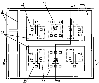
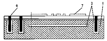
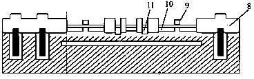
[0038] A field effect tube chip array thermoelectric converter, such as figure 1 , Figure 2A , Figure 2B , Figure 2C , Figure 3A , Figure 3B As shown, it includes a P-type silicon substrate 1, a silicon island 13, a boron-doped silicon layer 2, a deep groove 5, polysilicon 6, a field oxide layer 8, and an etched groove 12. The P-type silicon substrate 1 is processed There are two silicon islands 13, and the P-type silicon substrate 1 is implanted with a boron-doped silicon layer 2 corresponding to the bottom of the area of ​​the silicon island 13. The P-type silicon substrate 1 is processed with square deep grooves 5 around the edge, and the left deep groove 5 A deep groove 5 parallel to it is processed beside it, and a rich boron-doped silicon layer 2 is injected into the deep groove 5, and the polysilicon 6 is filled in the deep groove 5, and the deep boron-doped silicon layer 2 is filled, and the deep groove 5 and the silicon island 13, The two silicon islands 13 ...

Embodiment 2

[0062] A field effect tube chip array thermoelectric converter, such as figure 1 , Figure 2A , Figure 2B , Figure 2C , Figure 3A , Figure 3B As shown, it includes a P-type silicon substrate 1, a silicon island 13, a boron-doped silicon layer 2, a deep groove 5, polysilicon 6, a field oxide layer 8, and an etched groove 12. The P-type silicon substrate 1 is processed There are two silicon islands 13, and the P-type silicon substrate 1 is implanted with a boron-doped silicon layer 2 corresponding to the bottom of the area of ​​the silicon island 13. The P-type silicon substrate 1 is processed with square deep grooves 5 around the edge, and the left deep groove 5 A deep groove 5 parallel to it is processed beside it, and a rich boron-doped silicon layer 2 is injected into the deep groove 5, and the polysilicon 6 is filled in the deep groove 5, and the deep boron-doped silicon layer 2 is filled, and the deep groove 5 and the silicon island 13, The two silicon islands 13 ...


PUM


Abstract

The invention belongs to the technical field with the bulk silicon micromechanical manufacturing technology and the silicon gate automatic alignment CMOS integrated circuit technology combined and particularly relates to an on-chip array thermoelectric converter of a field effect transistor and a fully-automatic alignment manufacturing technology of the on-chip array thermoelectric converter. To solve the technical problems, the on-chip array thermoelectric converter of the field effect transistor is provided and comprises a P-type silicon substrate, silicon islands, heavy boron doped silicon layers, deep grooves, heavy boron doped silicon layers in the deep grooves, polycrystalline silicon and field region oxide layers. The two silicon islands are machined on the P-type silicon substrate, the heavy boron doped silicon layers are injected into the bottoms of the regions, corresponding to the silicon islands, of the P-type silicon substrate, the square deep grooves are formed in the peripheral edges of the P-type silicon substrate, the heavy boron doped silicon layers are injected into the deep grooves, the deep grooves are filled with the polycrystalline silicon, and the deep grooves and the silicon islands as well as the silicon islands are connected through the field region oxide layers. The on-chip array thermoelectric converter of the field effect transistor has the advantages of being high in response speed, wide in measurement frequency band, excellent in dynamic and overload characteristic and novel in structure.

Description

technical field [0001] The invention belongs to the technical field of the combination of bulk silicon micromachine manufacturing technology and silicon gate self-alignment CMOS integrated circuit technology, and specifically relates to an array thermoelectric converter on a field effect tube chip and its full self-alignment manufacturing technology. Background technique [0002] The traditional thermoelectric converter converts the electrical power to be measured generated by the product of voltage and current into Joule heat through a heating resistor. Then, the temperature change of the heating resistor is sensed by a thermocouple temperature measuring element and a voltage signal is output. This kind of thermoelectric converter has various forms, the conversion principle conforms to the original definition of electric power, the detection process has the compensation principle, and the accuracy is better than 0.1%. In this traditional thermoelectric converter, although ...

Claims


Application Information

Patent Timeline
Patent Type & Authority Applications(China)
IPC IPC(8): H01L35/00H01L35/34
Inventor 袁寿财谢晓春韩建强袁新娣廖昱博
Owner GANNAN NORMAL UNIV
Why Eureka
Try Eureka