Supercharge Your Innovation With Domain-Expert AI Agents!

Method for manufacturing through-hole silicon via

一种穿透硅通孔、制造方法的技术,应用在半导体/固态器件制造、电气元件、电固体器件等方向,能够解决出现裂缝、功率损失增加、穿透硅通孔隔离难等问题,达到简单制造的效果

Inactive Publication Date: 2016-04-13
SK HYNIX INC
View PDF3 Cites 0 Cited by
  • Summary
  • Abstract
  • Description
  • Claims
  • Application Information

AI Technical Summary

Problems solved by technology

[0013] At this time, if the thickness of the oxidized part is uneven or thin, cracks (leak) may appear
Also, when the through-silicon via is penetrated to have a structure including a conductive substance, an oxide film, and silicon and operates as a metal-oxide-semiconductor (MOS), problems such as an increase in power loss (insertion loss) may occur due to an increase in capacitance. Negative impact
[0014] In particular, it becomes more difficult to isolate the sides of TSVs when the aspect ratio (aspectratio) is large

Method used


Image

  • Method for manufacturing through-hole silicon via
  • Method for manufacturing through-hole silicon via
  • Method for manufacturing through-hole silicon via

Examples


Embodiment Construction

[0029] Hereinafter, the present invention will be described in more detail with reference to the accompanying drawings.

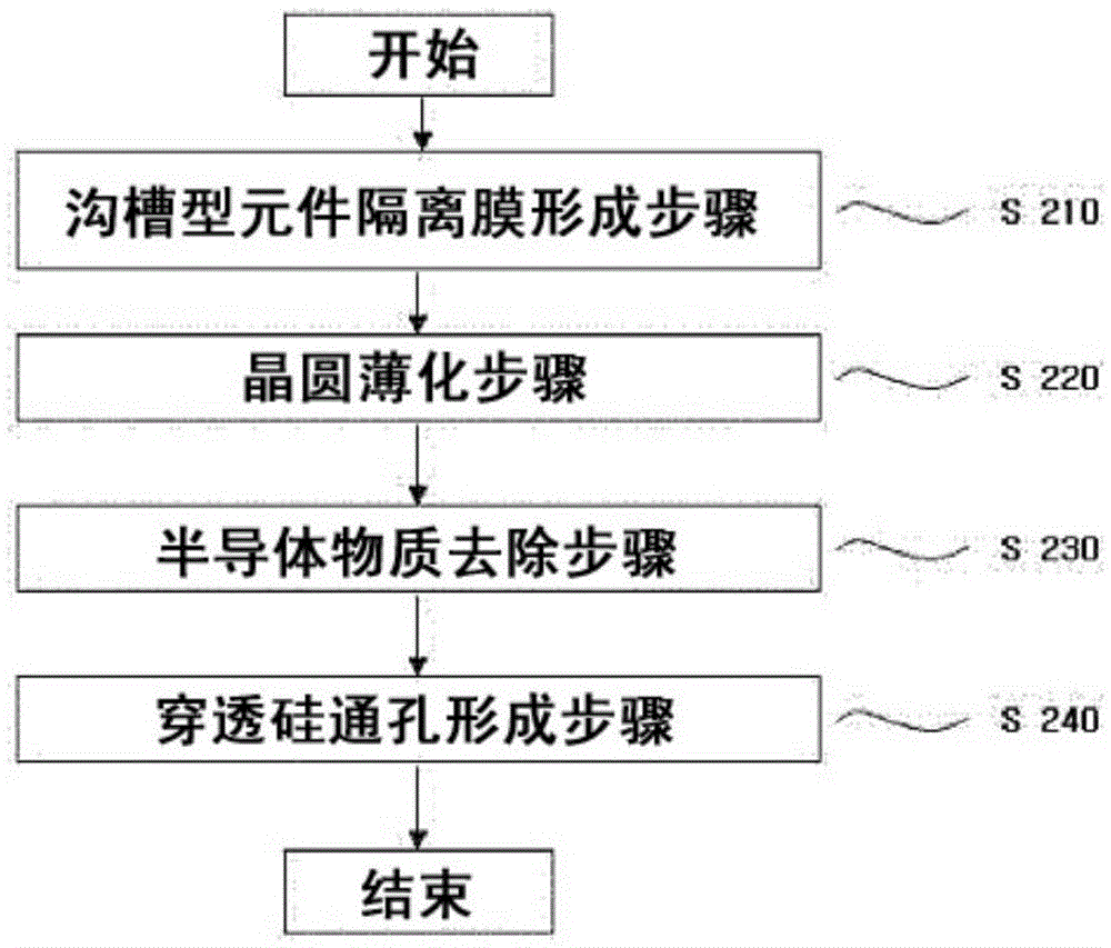
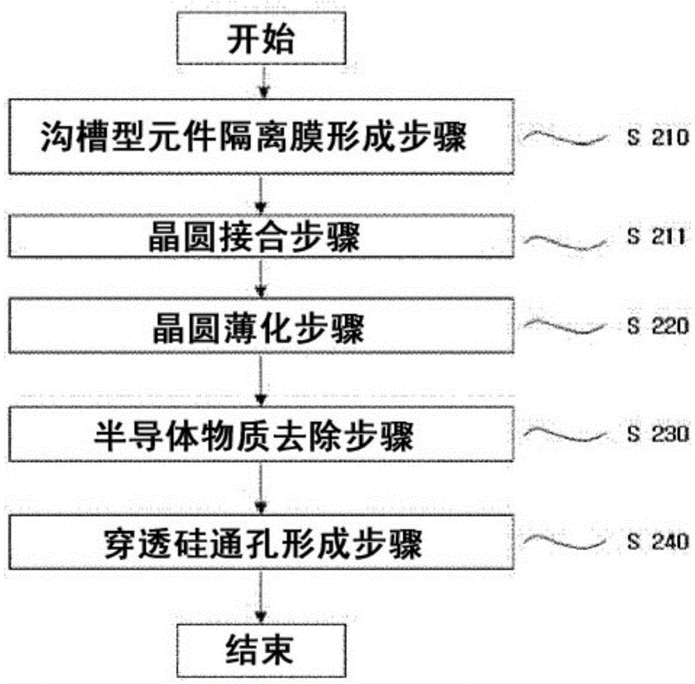
[0030] Figure 2 to Figure 3 It is a process flow diagram showing a manufacturing method of a TSV according to an embodiment of the present invention.

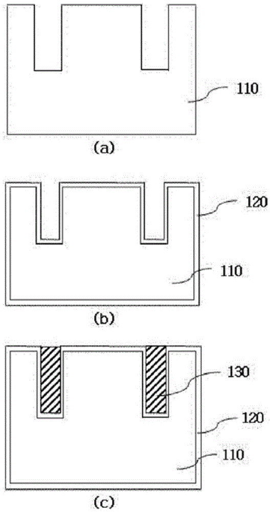
[0031] refer to figure 2 , the manufacturing method of the TSV according to an embodiment of the present invention includes the step of forming a trench-type device isolation film (S210), the step of wafer thinning (S220), the step of removing semiconductor substances (S230) and the step of TSV Hole forming step (S240).

[0032] Firstly, the step of forming a trench-type device isolation film ( S210 ) is to form a trench-type device isolation film on the first wafer by using a trench-type device isolation process.

[0033] That is, a trench-type element isolation film is formed at the position where the TSV is to be formed by using a trench-type element isolation process.

[0034] At this time, the tre...


PUM

PropertyMeasurementUnit
aspect ratioaaaaaaaaaa

Abstract

The present invention relates to a method for manufacturing a through-hole silicon via (TSV), and the method for manufacturing a through-hole silicon via (TSV) employs the conventional trench insulation process to readily manufacture a through-hole silicon via (TSV) with achievement of an effective electrical insulation between the through-hole silicon via (TSV) and the silicon.

Description

technical field [0001] The present invention relates to a method for manufacturing through-silicon vias (TSVs), and more particularly, relates to a method for simply manufacturing through-silicon vias by using the existing trench-type component isolation process, and completing through-silicon vias. Method for fabricating through-silicon vias for effective electrical isolation between holes and silicon substrates. Background technique [0002] The three-dimensional stack package in the packaging technology of semiconductor integrated circuits is a package in which a plurality of chips with the same storage capacity are stacked, and is generally called a stack chip package (StackChipPackage). [0003] Stacked chip packaging technology has the advantages of being able to stack chips with a simple process to improve packaging performance, reduce production costs, and facilitate mass production. On the contrary, it also has the advantages of increasing the number and size of sta...

Claims


Application Information

Patent Timeline
Patent Type & Authority Applications(China)
IPC IPC(8): H01L23/48H01L23/12
CPCH01L21/76898H01L23/12H01L23/48H01L21/30604H01L21/6835H01L21/7684H01L2221/68327H01L2221/68359
Inventor 安熙均安相旭李龙云郑喜灿李道永
Owner SK HYNIX INC
Features
  • R&D
  • Intellectual Property
  • Life Sciences
  • Materials
  • Tech Scout
  • Unparalleled Data Quality
  • Higher Quality Content
  • 60% Fewer Hallucinations
Learn More