
Fully wafer-level packaged mems microphone and manufacturing method thereof

A wafer-level packaging and manufacturing method technology, applied in the field of microphones, can solve the problems of particle and organic pollution that are not easy to avoid, the MEMS packaging structure is not compact, and the performance consistency cannot be guaranteed, and achieves improved mechanical robustness, good performance matching, The effect of low yield loss

Active Publication Date: 2020-05-15
GOERTEK MICROELECTRONICS CO LTD
View PDF7 Cites 0 Cited by
  • Summary
  • Abstract
  • Description
  • Claims
  • Application Information

AI Technical Summary

Problems solved by technology

In particular, when the package size is further reduced according to the trend, the package cost will become the bottleneck of cost reduction
Second, it is not conducive to manufacturing and mass production, because a single MEMS microphone chip needs to be individually packaged
Third, performance consistency cannot be guaranteed, and particle and organic pollution are not easy to avoid
Fourth, due to the non-compact structure of this MEMS package, its size reduction is greatly limited
However, this U.S. patent application only discloses the chip structure of the MEMS microphone and the wafer process flow for manufacturing the structure, which is not actually a packaged MEMS microphone that can be surface-mounted, and still requires traditional acoustics after the wafer process. encapsulation
Therefore, fully wafer-level packaged MEMS microphones, which are fully packaged at the wafer level and do not require any further processing after wafer dicing, and methods of manufacturing the same remain unapplied.

Method used


Image

  • Fully wafer-level packaged mems microphone and manufacturing method thereof
  • Fully wafer-level packaged mems microphone and manufacturing method thereof
  • Fully wafer-level packaged mems microphone and manufacturing method thereof

Examples


Embodiment Construction

[0026] Aspects of the claimed subject matter are described below with reference to the accompanying drawings, in which the figures are schematic and not drawn to scale, and like reference numerals are used to refer to like elements throughout. . In the following description, for purposes of explanation, numerous specific details are set forth in order to provide a thorough understanding of one or more aspects. It may be evident, however, that these aspects may be practiced without these specific details. In other instances, well-known structures and devices are shown in block diagram form in order to facilitate describing one or more aspects.

[0027] In the specification and appended claims, it should be understood that when a layer, region, or element is referred to as being "on" or "under" another layer, region, or element, it It may be "directly" or "indirectly" on or under the other layer, region, or component, or one or more intervening layers may also be present.

[...


PUM


Abstract

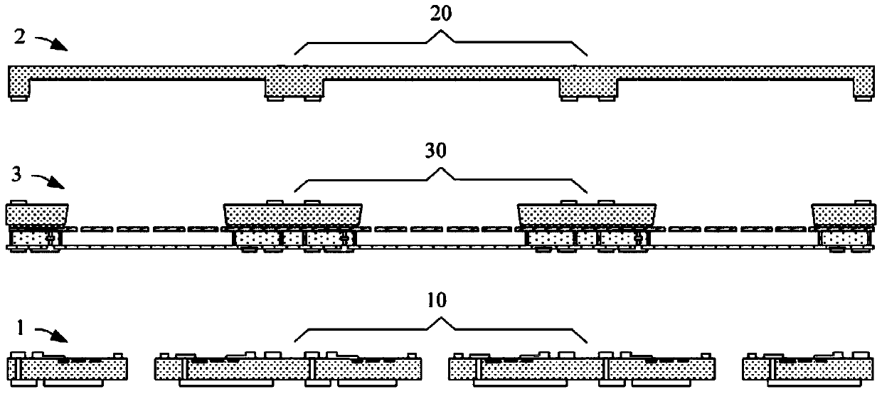
The present invention provides a method for manufacturing a fully wafer-level packaged MEMS microphone and the manufactured microphone. The method includes: respectively manufacturing a first packaged chip, a MEMS microphone chip and a second packaged chip; Wafer-to-wafer bonding to form a plurality of fully wafer-level packaged MEMS microphone units; dicing the fully wafer-level packaged MEMS microphone units to form a plurality of fully wafer-level packaged MEMS microphones fully in Packaging is performed at the wafer level and does not require any further processing after wafer dicing. The method can improve cost-effectiveness, performance consistency, manufacturability, quality, scalability of the packaged MEMS microphone.

Description

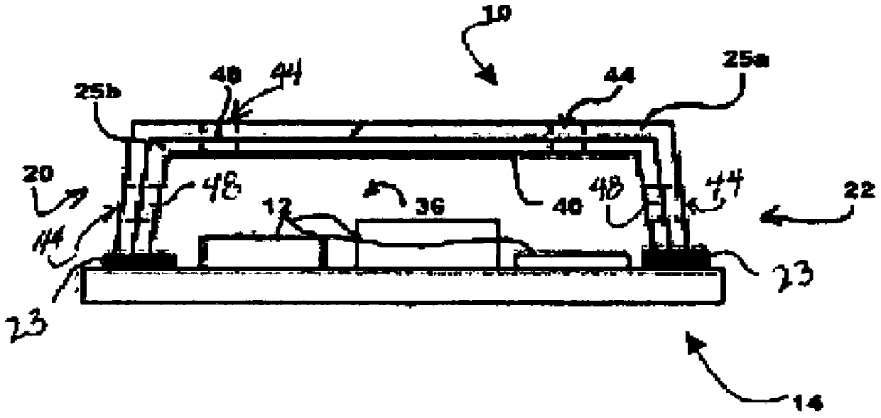
technical field [0001] The present invention relates to the technical field of microphones, more specifically, to a packaged MEMS microphone and a manufacturing method thereof. Background technique [0002] Silicon-based MEMS (micro-electro-mechanical systems) microphones, also known as acoustic transducers, are playing an increasingly important role in hearing aids, mobile communication systems, digital still and video cameras, and in the toy industry. Typically, silicon-based MEMS microphone chips need to be packaged before they can be tested, shipped and used. US Patent 6,781,231 discloses a method such as figure 1 A typical MEMS package is shown, which includes a surface-mountable component 12 (e.g., a silicon-based MEMS microphone chip, an integrated circuit), a substrate 14, and a cover 20, wherein the substrate 14 and cover 20 are combined to form a housing 22 , the surface-mountable component 12 is located in the housing 22 and electrically connected. [0003] How...

Claims


Application Information

Patent Timeline
Patent Type & Authority Patents(China)
IPC IPC(8): H04R19/04H04R31/00
CPCH04R19/04H04R31/00H04R2201/003B81C1/00888B81B2207/07B81C2203/0792B81B2201/0257B81B2203/04B81B2207/012B81C2203/0118B81C2203/058B81B7/00B81B3/001B81B2203/0127B81C1/0023B81C2203/0785H04R19/005H04R31/006
Inventor 邹泉波王喆
Owner GOERTEK MICROELECTRONICS CO LTD
Learn More