Integrated circuit layout optimizing method based on side-denoted short-circuit critical area network
A key area and optimization method technology, applied in the field of microelectronics, can solve the problems of inaccurate optimization results, failure to consider the impact, and inability to accelerate optimization, etc., to achieve the effects of reducing space complexity, layout optimization, and defect rate
- Summary
- Abstract
- Description
- Claims
- Application Information
AI Technical Summary
Problems solved by technology
Method used
Image
Examples
Embodiment Construction
[0043] The specific implementation steps of the present invention will be further described in detail below in conjunction with the figures.
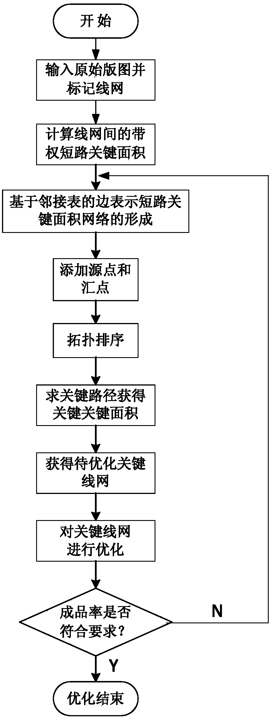
[0044] According to attached figure 1 , realize the steps of the inventive method as follows:
[0045] Step 1. Input the original layout and mark the net
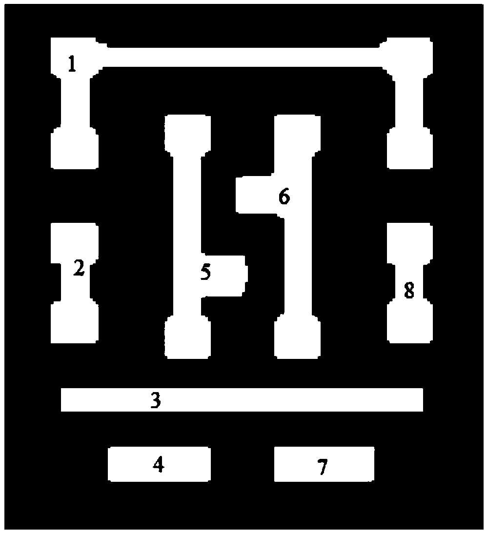
[0046] Input a layout image as the source image, use the matlab library function to convert the source image into a binary image, and then assign numbers to each connected area in the binary image in increasing order, that is, to number each line network. Such as figure 2 as shown, figure 2is the converted binary plane layout, which has 8 connected regions, that is, 8 nets, which are numbered 1...8 in columns;
[0047] Step 2. Calculate the weighted short-circuit critical area between nets
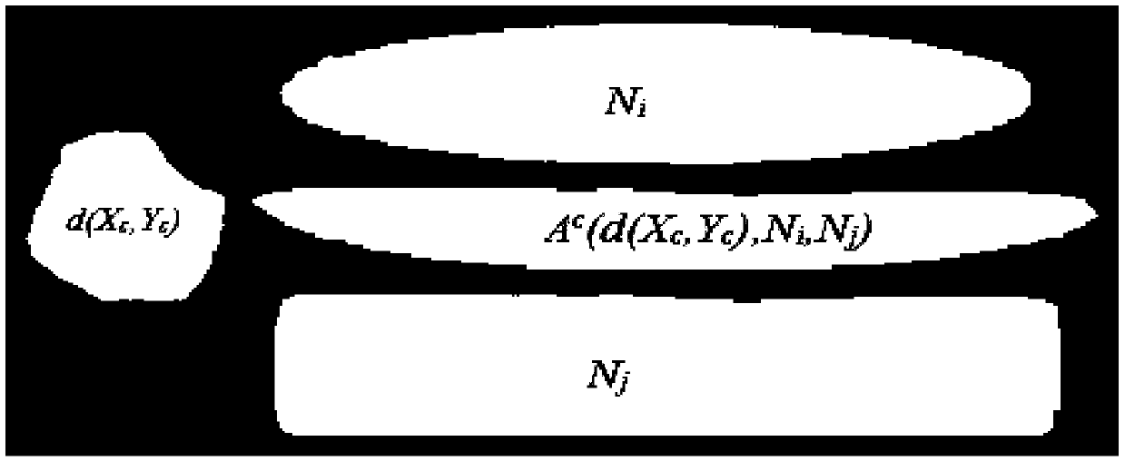
[0048] Such as image 3 shown, for n i row m i Arbitrarily shaped line network N of columns i and n j row m j Arbitrary shape line network N of columns j , where i,j=1,2,...8, i ima...
PUM
 Abstract
Description
Claims
Application Information


