
Insulated gate bipolar transistor

A bipolar transistor and insulated gate technology, applied in semiconductor devices, electrical components, circuits, etc., can solve the problems of high conduction voltage drop and long switching time

Inactive Publication Date: 2016-04-20
WENZHOU MOSHANG MICROELECTRONICS CO LTD
View PDF4 Cites 2 Cited by
  • Summary
  • Abstract
  • Description
  • Claims
  • Application Information

AI Technical Summary

Problems solved by technology

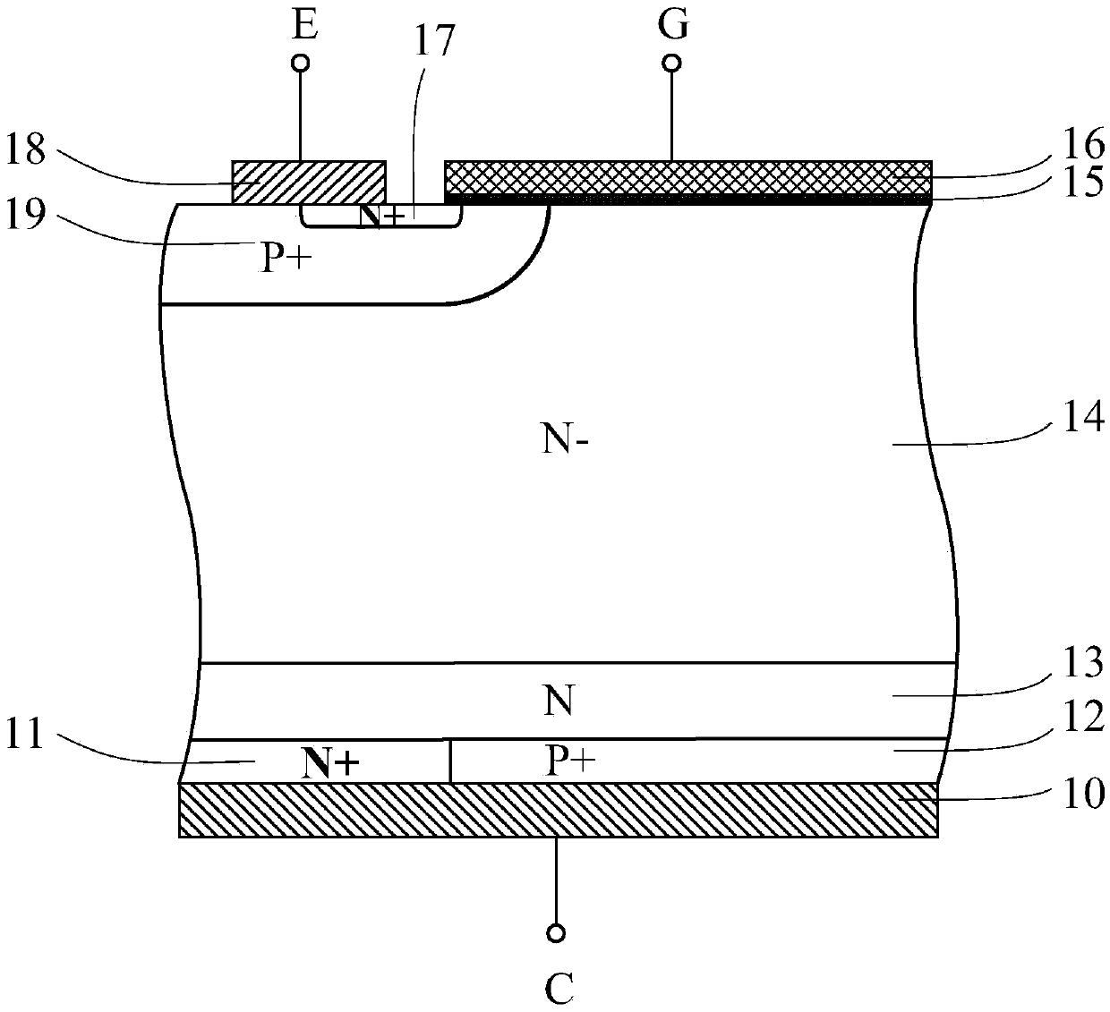
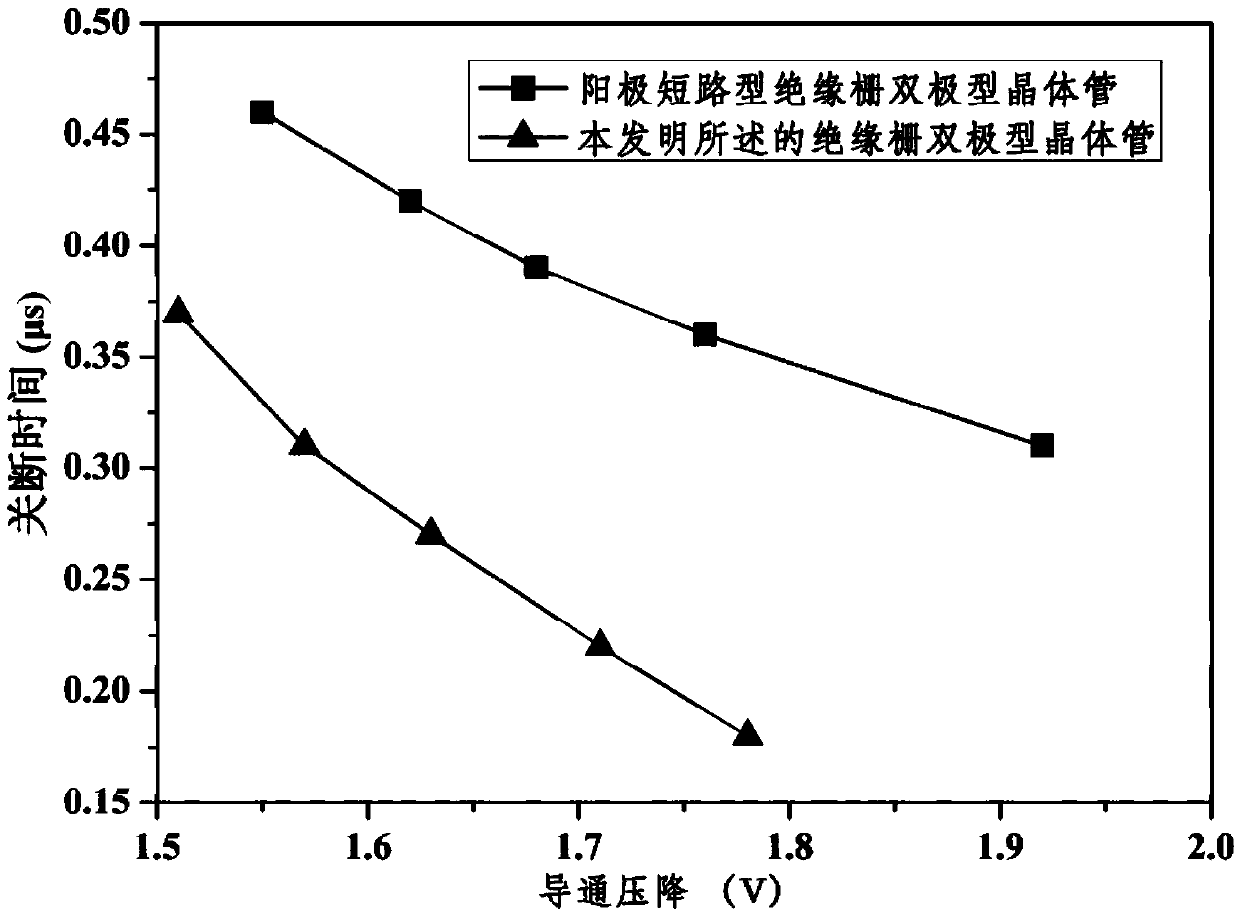
[0005] In order to overcome the problem that the conduction voltage of the existing traditional insulated gate bipolar transistor is reduced but the switching time is long, and the anode short-circuit type insulated gate bipolar transistor has a high switching speed but a high conduction voltage drop, it provides a Fast switching insulated gate bipolar transistor with a good compromise between on-voltage drop and switching time

Method used


Image

  • Insulated gate bipolar transistor
  • Insulated gate bipolar transistor
  • Insulated gate bipolar transistor

Examples


Embodiment Construction

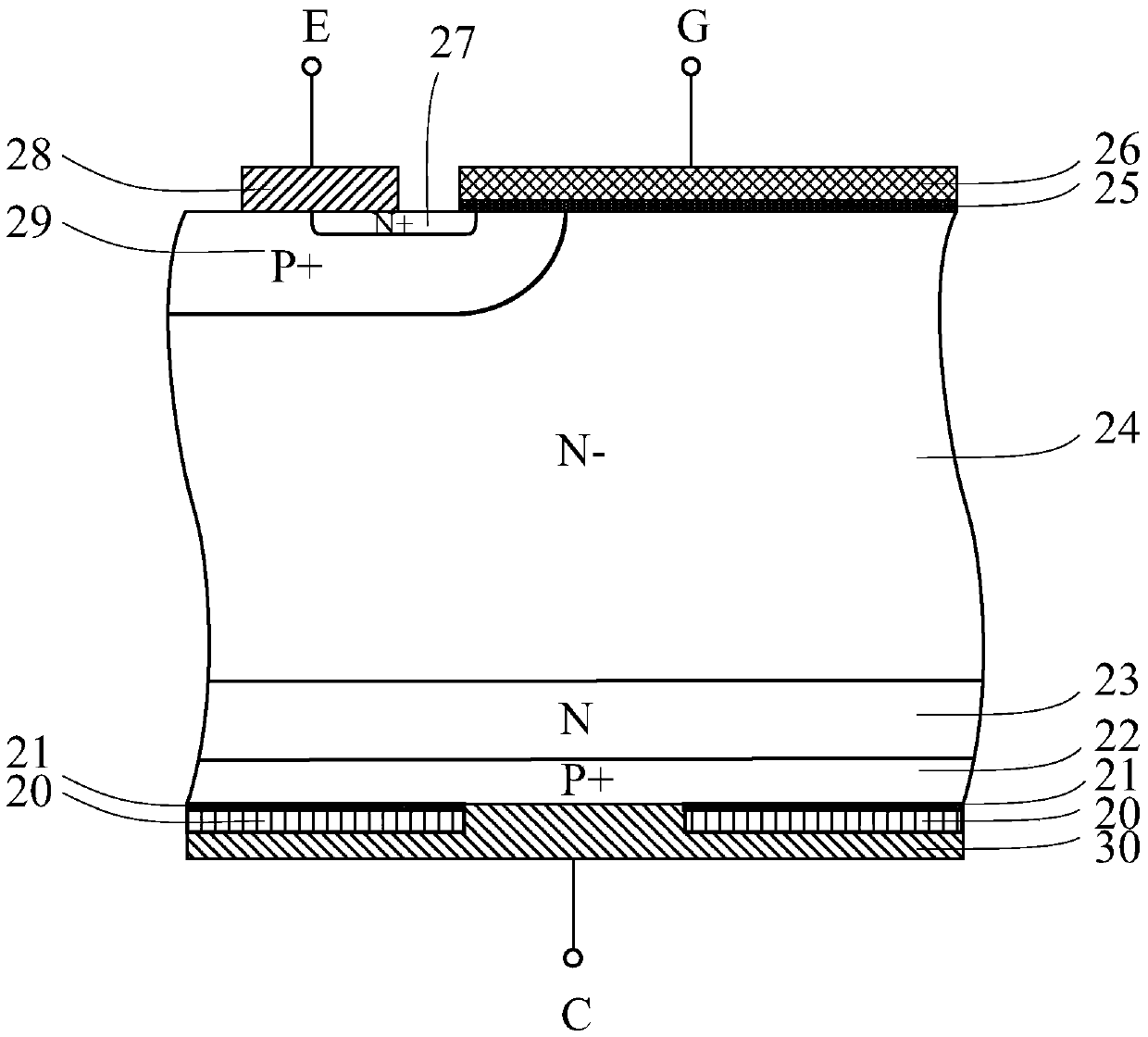
[0017] Such as figure 2 As shown, the insulated gate bipolar transistor provided in this embodiment includes: N-base region 24, P+ base region 29, N+ emitter region 27, emitter 28, gate oxide layer 25, gate electrode 26, N-type buffer Layer 23, P+ collector region 22, thin silicon dioxide layer 21, N-type polysilicon region 20 and metal collector 30, characterized in that: P+ base region 29, N+ emitter region 27, emitter 28, gate oxide layer 25 With the gate electrode 26 on one side of the N-base region, the N-type buffer layer 23, the P+ collector region 22, the thin silicon dioxide layer 21, the N-type polysilicon region 20 and the metal collector 30 are on the other side of the N-base region 24 One side; the N-type buffer layer 23 and the P+ collector region 22 are sequentially stacked away from the N-base region 24; the thin silicon dioxide layer 21 and the N-type polysilicon region 20 are formed from the P+ collector region 22 to The direction away from the N-type buffe...


PUM

PropertyMeasurementUnit
Thicknessaaaaaaaaaa
Thicknessaaaaaaaaaa

Abstract

The invention discloses an insulated gate bipolar transistor, and the transistor comprises an N- base region, a P+ base region, an N+ emitter region, an emitter region, a gate oxide layer, a gate electrode, an N-type buffering layer, a P+ collector region, a thin silicon dioxide layer, an N-type polycrystalline silicon region, and a collector electrode. The transistor is characterized in that the P+ base region, the N+ emitter region, the emitter region, the gate oxide layer and the gate electrode are located at one side of the N- base region; the N-type buffering layer, the P+ collector region, the thin silicon dioxide layer, the N-type polycrystalline silicon region and the collector electrode are located at the other side; the thin silicon dioxide layer and the N-type polycrystalline silicon region are sequentially stacked through the P+ collector region to form a polycrystalline silicon emitter region which does not cover the P+ collector region completely. The N-type buffering layer, the P+ collector region and the polycrystalline silicon emitter region form a quick switching polycrystalline silicon emitter NPN-type triode, thereby forming a non-balance carrier extraction quick channel during the switching-off of the transistor, and facilitating the quick switching of the transistor.

Description

technical field [0001] The invention relates to the technical field of semiconductor power devices, in particular to an insulated gate bipolar transistor. Background technique [0002] Insulated Gate Bipolar Transistor (Insulated Gate Bipolar Transistor, referred to as IGBT) is a rapidly developing and widely used semiconductor power device. It can be regarded as a composite fully-controlled semiconductor power device composed of a metal oxide semiconductor field effect transistor (MOSFET) and a bipolar junction transistor (BJT). It not only has the advantages of power MOSFET voltage control, high input impedance, and simple driving circuit, but also has many advantages such as small on-resistance, high current density, and high blocking voltage of BJT. It is widely used in household appliances, new energy power generation, smart grid, power traction and other fields. [0003] As we all know, when the insulated gate bipolar transistor is forward-conducting, the collector o...

Claims


Application Information

Patent Timeline
IPC IPC(8): H01L29/06H01L29/08H01L29/739
CPCH01L29/7398H01L29/0684H01L29/0804H01L29/0821
Inventor 程维维张斌魏可情吴泉鑫李伟铭张成洲林云斌朱佳甘露唐雪梅
Owner WENZHOU MOSHANG MICROELECTRONICS CO LTD
Learn More