Quantum dot light-emitting diode sub-pixel array, manufacturing method thereof and display device

A quantum dot light-emitting and sub-pixel technology, which is applied in semiconductor/solid-state device manufacturing, electrical components, circuits, etc., can solve problems such as high technical difficulty, high commodity prices, and low product yield, and achieve improved process yield and cost. The effect of reducing and facilitating the preparation

Active Publication Date: 2016-04-20
BOE TECH GRP CO LTD
View PDF5 Cites 21 Cited by
  • Summary
  • Abstract
  • Description
  • Claims
  • Application Information

AI Technical Summary

Problems solved by technology

Therefore, high-resolution AMOLED products face serious problems of hi

Method used


Image

  • Quantum dot light-emitting diode sub-pixel array, manufacturing method thereof and display device
  • Quantum dot light-emitting diode sub-pixel array, manufacturing method thereof and display device
  • Quantum dot light-emitting diode sub-pixel array, manufacturing method thereof and display device

Examples


no. 1 example

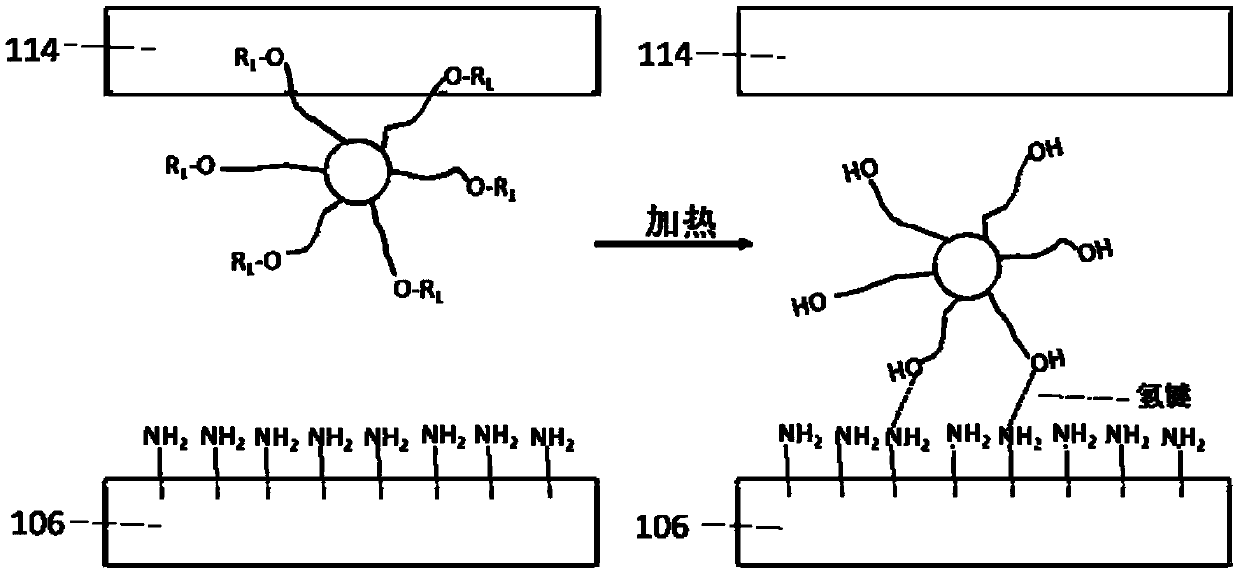
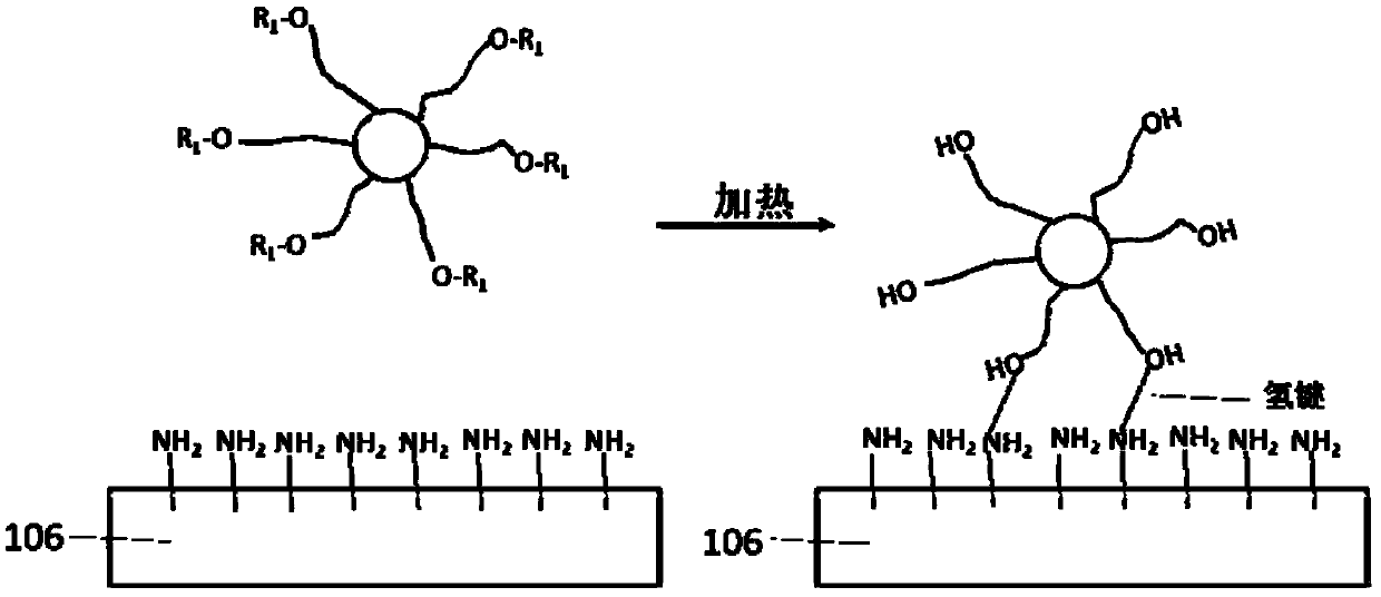
[0061] Figure 2A-2K It is a schematic diagram illustrating each stage of the method for preparing a quantum dot light emitting diode sub-pixel array according to the first embodiment of the present invention through cross-sectional views. In a specific example, for example, the green, blue, and red quantum dot light-emitting diode sub-pixel arrays can be separately prepared on the substrate by a laser heating method.

[0062] First of all, Figure 2A The initial structure of this embodiment is shown. The initial structure is the base substrate 202, the material of which is well known in the art, such as glass or quartz. The base substrate 202 may be transparent or opaque. The base substrate 202 is cleaned using standard methods.

[0063] Next, like Figure 2B As shown, an optional thin film transistor (TFT) array 204 is prepared on a base substrate 202. The specific manufacturing method and structure of the TFT array are not limited, and they can be methods and structures known...

no. 2 example

[0086] In the second embodiment, a method similar to the first embodiment is used to independently realize the transfer of each thermally sensitive quantum dot material layer to the corresponding sub-pixel area. The difference between the second embodiment and the first embodiment is that instead of using the carrier substrate of the thermally sensitive quantum dot material layer, a thermally conductive mask is directly used to carry the thermally sensitive quantum dot material. In the following description, the parts in the second embodiment that are similar to those in the first embodiment will not be described in detail.

[0087] Figure 3A-3H It is a schematic diagram illustrating each stage of the method for preparing a quantum dot light emitting diode sub-pixel array according to the second embodiment of the present invention through cross-sectional views.

[0088] Such as Figure 3A with 3B As shown, an optional TFT array 304 is prepared on the cleaned base substrate 302, an...

no. 3 example

[0104] In the third embodiment, a heating method similar to the first embodiment is used to independently realize the transfer of each thermally sensitive quantum dot material layer to the corresponding sub-pixel area. The main difference between the third embodiment and the first embodiment is that instead of using the carrier substrate of the thermally sensitive quantum dot material layer, the thermally sensitive quantum dot material layer is directly coated on the quantum dot receiving layer. In the following description, the parts in the third embodiment that are similar to those in the first embodiment will not be described in detail.

[0105] Figure 4A-4H It is a schematic diagram illustrating each stage of the method for preparing a quantum dot light emitting diode sub-pixel array according to the third embodiment of the present invention through cross-sectional views.

[0106] Such as Figure 4A with 4B As shown, an optional TFT array 404 is prepared on the cleaned base su...


PUM

PropertyMeasurementUnit
Thicknessaaaaaaaaaa
Resolutionaaaaaaaaaa

Abstract

The embodiment of the invention relates to a manufacturing method of a quantum dot light-emitting diode sub-pixel array, the quantum dot light-emitting diode sub-pixel array manufactured through the method and a display device including the quantum dot light-emitting diode sub-pixel array. The manufacturing method of the quantum dot light-emitting diode sub-pixel array includes a quantum dot receiving layer forming step, a heat-sensitive quantum dot material layer applying step and a heat-sensitive quantum dot material transferring step. According to the quantum dot receiving layer forming step, a quantum dot receiving layer is formed on a substrate. According to the heat-sensitive quantum dot material layer applying step, a heat-sensitive quantum dot material layer is applied to the quantum dot receiving layer, wherein the heat-sensitive quantum dot material layer comprises heat-sensitive organic ligands. According to the heat-sensitive quantum dot material transferring step, the organic ligands of a heat-sensitive quantum dot material in the preset region of the heat-sensitive quantum dot material layer are subjected to a chemical reaction through heating, and then the heat-sensitive quantum dot material in the preset region is transferred to corresponding sub-pixel regions on the quantum dot receiving layer.

Description

Technical field [0001] The embodiments of the present invention generally relate to the field of display devices, and in particular, to a method for manufacturing a quantum dot light-emitting diode sub-pixel array, a quantum dot light-emitting diode sub-pixel array manufactured thereby, and a display device including the quantum dot light-emitting diode sub-pixel array. Background technique [0002] Active matrix organic light-emitting diodes (AMOLED) were once recognized as promising as the next generation of display products to replace liquid crystal displays (LCD). However, with the improvement of consumer consumption levels, high-resolution products have become the key development direction of display products, and high-resolution AMOLED products are difficult to compete with LCD. This is because the organic layer structure of organic light-emitting display products usually uses masks. However, the mask evaporation method has the disadvantages of difficulty in alignment, low ...

Claims


Application Information

Patent Timeline
IPC IPC(8): H01L51/56H01L51/52H01L51/54H01L27/32
CPCH10K59/00H10K85/00H10K50/80H10K71/00H10K59/35H10K71/162H10K71/18H10K71/211H10K71/80H10K50/115H10K71/40H10K85/342H10K71/421H10K50/15H10K50/16H10K85/30H10K85/111H10K85/115H10K85/1135
Inventor 李延钊鲍里斯·克里斯塔尔钟杰兴王龙陈卓
Owner BOE TECH GRP CO LTD
Why Eureka
Try Eureka