Low-temperature-resistant display device

A technology for display devices and liquid crystal layers, applied in instruments, nonlinear optics, optics, etc., can solve problems such as tailing of liquid crystal displays

Inactive Publication Date: 2016-05-11
BOE TECH GRP CO LTD +1
View PDF5 Cites 11 Cited by
  • Summary
  • Abstract
  • Description
  • Claims
  • Application Information

AI Technical Summary

Problems solved by technology

Therefore, in a low temperature environment, the liquid crystal display will smear when switching screens or scanning display.

Method used


Image

  • Low-temperature-resistant display device
  • Low-temperature-resistant display device
  • Low-temperature-resistant display device

Examples


Embodiment 1

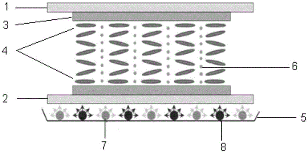
[0023] Embodiment 1 A display device

[0024] This embodiment provides a display device including a TFT substrate 1, a CF substrate 2, an alignment film layer 3, a liquid crystal layer 4, and a backlight 5; wherein, a near-infrared light absorber 6 is added to the liquid crystal layer 4, and Visible light emitting diodes 7 and near-infrared light emitting diodes 8 are integrated in the backlight source.

[0025] The near-infrared light absorber is specifically a squaraine dye (a kind of near-infrared light absorber cyanine dyes), which is evenly distributed in the alignment film layer, and the addition amount of the squaraine dye is specifically 0.01% of the mass of the alignment film ~0.1% (mass wt%, calculated based on the total mass of the alignment film used in a single panel).

[0026] The near-infrared light-emitting diode is composed of a GaAs compound semiconductor light-emitting diode and a polarizer, and the wavelength of the near-infrared light emitted by it is ≤ 3 micron...

Embodiment 2

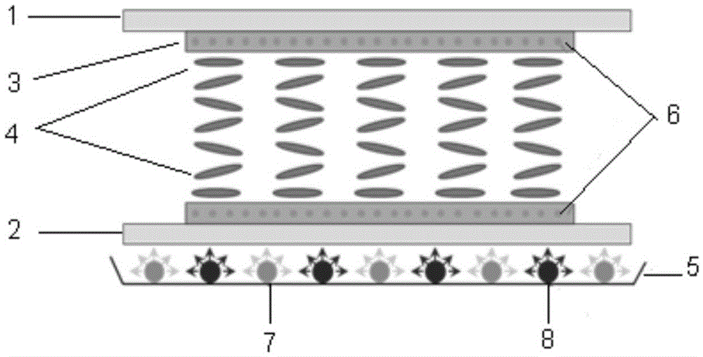
[0028] Embodiment 2 A display device

[0029] This embodiment provides a display device, the structure is basically similar to that of Embodiment 1, and the difference lies in:

[0030] The near-infrared light absorber is specifically a squaraine dye (a kind of near-infrared light absorber cyanine dye), which is uniformly distributed in the liquid crystal layer, and the addition amount of the squaraine dye is specifically 0.01% to 0.1% of the mass of the liquid crystal (Weight% by mass, calculated based on the total mass of liquid crystal used in a single panel).

Embodiment 3

[0032] This embodiment provides a display device, the structure is basically similar to that of Embodiment 1, and the difference lies in:

[0033] The near-infrared light absorber is specifically a squaraine dye (a kind of near-infrared light absorber cyanine dye), which is uniformly distributed in the alignment film layer and the liquid crystal layer, wherein the amount of the squaraine dye added in the alignment film layer It is 0.01% to 0.1% of the mass of the alignment film, and the addition amount of squaraine dye in the liquid crystal layer is 0.01% to 0.1% of the mass of the liquid crystal (mass wt%, according to the total mass of the alignment film used in a single panel and the total mass of the liquid crystal respectively Calculation).


PUM

PropertyMeasurementUnit
particle sizeaaaaaaaaaa
sizeaaaaaaaaaa

Abstract

The invention relates to a display device. The display device comprises an array substrate, an alignment film layer, a liquid crystal layer and a backlight source, wherein the liquid crystal layer and / or the alignment film layer contain and / or contains a near-infrared light absorbent, and near-infrared light diodes are arranged in the backlight source. According to the display device, by emitting certain near-infrared light with a specific wavelength to TFT-LCD, the light absorbed by the substrate is reduced; most near-infrared light penetrating through the substrate is absorbed by the liquid crystal layer or the alignment film layer, and then the liquid crystal layer is heated, so that the response speed of a liquid crystal display at a low-temperature environment is increased, and the stability of electronic equipment is enhanced; the trailing problem occurring in a screen switching process or a scan display process of the display device at the low-temperature environment is solved.

Description

Technical field [0001] The invention relates to a novel low temperature resistant display device, which belongs to the technical field of liquid crystal display. Background technique [0002] A common TFT-LCD includes a TFT substrate, an alignment film layer on each substrate, a liquid crystal, and a backlight structure. Ordinary TFT-LCD has a slower response speed in a low-temperature environment, mainly because when the temperature of the liquid crystal molecules is low, the activity energy of the molecules is weakened, and the viscosity coefficient of the corresponding liquid crystal material becomes larger. When an electric field is applied to the liquid crystal molecules, the viscous resistance of the liquid crystal molecules is relatively large, and it takes a long time to reach the desired twist angle. Therefore, in a low temperature environment, the liquid crystal display has a tailing phenomenon when switching screens or scanning displays. Summary of the invention [00...

Claims


Application Information

Patent Timeline
Patent Type & Authority Applications(China)
IPC IPC(8): G02F1/1333G02F1/1337G02F1/13357
CPCG02F1/1333G02F1/133603G02F1/1337G02F2201/083
Inventor 胡滕滕任锦宇周波
Owner BOE TECH GRP CO LTD
Why Eureka
Try Eureka