
Array substrate, touch screen, touch display device and manufacturing method thereof

A technology for array substrates and display areas, applied to static indicators, instruments, semiconductor devices, etc., can solve the problems of increasing costs, difficulty of preparation process, and affecting the performance of metal oxide semiconductors, so as to reduce production costs and increase stability , reducing the effect of the mask

Active Publication Date: 2016-05-11
SHANGHAI TIANMA MICRO ELECTRONICS CO LTD +1
View PDF3 Cites 28 Cited by
  • Summary
  • Abstract
  • Description
  • Claims
  • Application Information

AI Technical Summary

Problems solved by technology

However, when the light energy is large, the light energy will still penetrate the protective layer and affect the back channel region, which will still affect the performance of metal oxide semiconductors.
[0006] The second is to use an opaque metal layer or multi-layer material as a light-shielding layer to cover the semiconductor channel area to prevent the impact of light on the stability of the semiconductor device: if you want to add a light-shielding layer, you need to make it through an additional mask, which is undoubtedly Will increase the cost and the difficulty of the preparation process

Method used


Image

  • Array substrate, touch screen, touch display device and manufacturing method thereof
  • Array substrate, touch screen, touch display device and manufacturing method thereof
  • Array substrate, touch screen, touch display device and manufacturing method thereof

Examples


Embodiment Construction

[0033] The present invention will be further described in detail below in conjunction with the accompanying drawings and embodiments. It should be understood that the specific embodiments described here are only used to explain the present invention, but not to limit the present invention. In addition, it should be noted that, for the convenience of description, only parts related to the present invention are shown in the drawings but not all content.

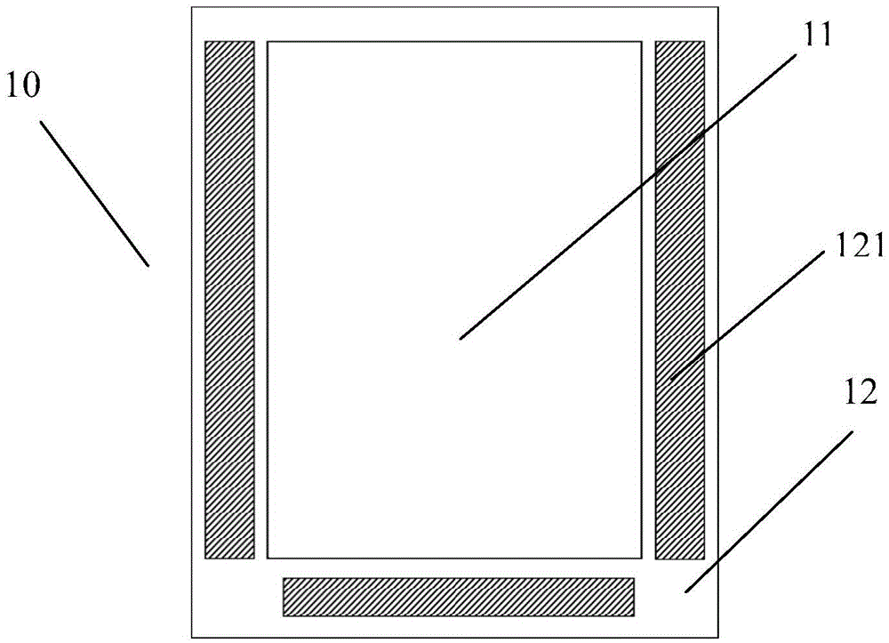
[0034] First, the present invention provides an array substrate, figure 1 A schematic diagram of an array substrate provided for an embodiment of the present invention, such as figure 1 As shown, the array substrate 10 includes a display area 11 for displaying images and a non-display area 12 at least on one side of the display area 11 . Alternatively, it can also be used as figure 1 As shown in , the non-display area 12 is located around the display area 11 .

[0035] The display area 11 of the array substrate includes a p...


PUM


Abstract

The invention provides an array substrate; a driving transistor of a peripheral driving circuit of the array substrate is a bigrid oxide semiconductor transistor; the top grid of the bigrid oxide semiconductor transistor and a touch lead positioned in a display area are formed in the same layer and made of the same material; and furthermore, the material of the top grid is non-transparent metal or alloy thereof having better conductivity, such as molybdenum, aluminium and copper. On the one hand, the bigrid oxide semiconductor transistor can be formed in the peripheral driving circuit in the event that an extra manufacturing process and a photomask are not increased, such that the purpose of controlling the threshold voltage of the oxide semiconductor transistor is realized; on the other hand, a lightproof metal layer is used as the top grid for covering a semiconductor channel region; and thus, photo-generated current can be reduced, such that influence of illumination on the stability of the oxide semiconductor transistor is avoided.

Description

technical field [0001] The present invention relates to the field of display technology, in particular to an array substrate integrated with a touch function, a manufacturing method thereof, a touch screen and a touch display device. Background technique [0002] In the field of liquid crystal display, active layers of thin film transistors have been using silicon-based materials with excellent properties such as stability and processability. Silicon-based materials are mainly divided into amorphous silicon and polycrystalline silicon. Among them, the mobility of amorphous silicon material is very low, and although polycrystalline silicon material has high mobility, the uniformity of devices manufactured with it is poor, the yield rate is low, and the unit price is high. . Therefore, in recent years, the technology of using transparent oxide semiconductor films for channel formation blocks to manufacture semiconductor active layers of devices such as thin film transistors (...

Claims


Application Information

Patent Timeline
Patent Type & Authority Applications(China)
IPC IPC(8): G06F3/041
CPCG06F3/0412G06F2203/04103H01L27/14609G06F3/044G06F3/04164G09G2310/0297G09G3/3659G09G2310/0262G09G3/36H01L27/124G09G2300/0426H10K59/12
Inventor 楼均辉吴天一吴勇
Owner SHANGHAI TIANMA MICRO ELECTRONICS CO LTD
Learn More