Method for preparing large-area and all-solid-state perovskite mesoscopic solar cell and product
A technology based on solar cells and perovskites, which is applied in the field of solar cells, can solve problems such as cell efficiency attenuation, extreme instability, and solar cell performance degradation, and achieve excellent performance, optimized layout, and improved filling performance.
- Summary
- Abstract
- Description
- Claims
- Application Information
AI Technical Summary
Problems solved by technology
Method used
Image
Examples
Embodiment 1
[0025] In this example, the specific process steps for preparing a large-area all-solid-state perovskite mesoscopic solar cell are as follows:
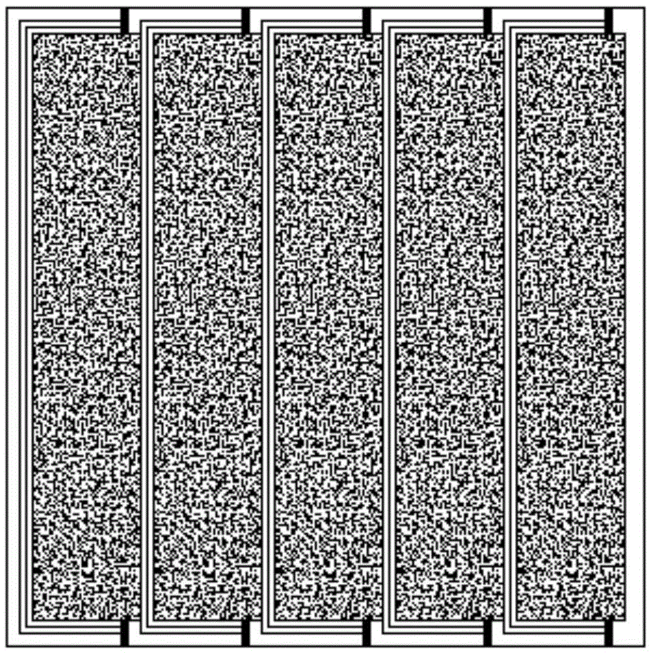
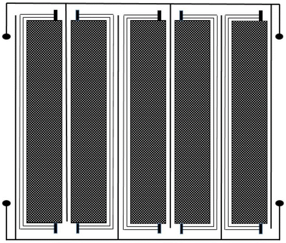
[0026] First, use a cutting machine to cut the conductive glass into glass sheets of a certain size. For example, the preferred size in this embodiment is 100mm×100mm, but it can also be other sizes. Use a laser to cut the conductive layer of the glass sheet at a certain distance from one of the edges. Etch an insulating strip parallel to the edge (preferably such as 5 mm from the edge in this embodiment), and etch a plurality of parallel insulating strips in the remaining area to divide the glass sheet into multiple regions, such as in this embodiment It is preferable to etch 4 parallel insulating strips again, thereby dividing the glass sheet into five positive electrode regions and negative electrode regions, so that the conductive layer cannot be completely conducted, and the etched glass sheet is ultrasonically cleaned with deterg...
Embodiment 2
[0035] In the present embodiment, different from Embodiment 1, the distance between the insulating tape and one edge of the glass sheet is preferably 3.5 mm, and the number of parallel insulating tape strips etched is preferably eight in the present embodiment, so that the glass sheet is divided into 8 areas to be printed that are not connected to each other.
[0036] Using screen printing technology, print a strip of silver paste parallel to the insulating tape on each area to be printed, the size can be the same as or different from the embodiment, for example, 0.5mm×100mm in this embodiment, and dry to form a metal wire . Print a layer of glass paste on the metal wires to completely cover the metal wires. After drying, it is sprayed on the surface of the glass sheet at 450°C to form a dense titanium dioxide film.
[0037] Correspondingly, print 8 titanium dioxide pastes on the dense titanium dioxide thin film layer, the size can be the same as that in Example 1, for examp...
Embodiment 3
[0041] In this embodiment, compared with Embodiment 2, the difference is that the number of parallel insulating strips etched is preferably ten in this embodiment, so that the glass sheet is divided into ten non-conductive regions to be printed. .
[0042] In addition, in the process of printing the silver paste parallel to the insulating tape, the size of the silver paste may be different from that in Embodiment 2, for example, the size of the silver paste in this embodiment is preferably 0.5mm×20mm. The spraying temperature of the titanium dioxide thin film may also be the same as or different from that in Embodiment 2. For example, the spraying temperature in this embodiment is 500° C., of course, the spraying temperature can be selected according to specific requirements.
[0043] The corresponding number of strips of titanium dioxide paste printed on the titanium dioxide thin film layer is 10, and the size may be different from that of Embodiment 2, for example, it is 5.5...
PUM
 Abstract
Description
Claims
Application Information

