Nickel-gold plating circuit board production technology

A production process and circuit board technology, applied in the direction of printed circuit, printed circuit manufacturing, electrical components, etc., can solve the problems of low production efficiency, unguaranteed quality of circuit board products, and high production cost, so as to improve production efficiency and sustain The effect of short production cycle and reduced loss

Active Publication Date: 2016-05-11
苏州市三生电子有限公司
View PDF4 Cites 1 Cited by
  • Summary
  • Abstract
  • Description
  • Claims
  • Application Information

AI Technical Summary

Problems solved by technology

[0002] In the circuit board production process, the conventional method is to adopt the following mode: circuit board appearance production --- circuit board appearance surface post-treatment --- punch hollowing --- nickel-gold pre-treatment --- nickel-gold treatment, no need In the cas...

Method used


Image

  • Nickel-gold plating circuit board production technology
  • Nickel-gold plating circuit board production technology
  • Nickel-gold plating circuit board production technology

Examples


Embodiment Construction

[0023] The present invention will be described in detail below with reference to the accompanying drawings and in combination with embodiments.

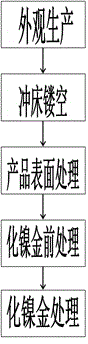
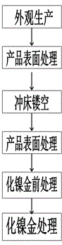
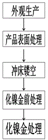
[0024] refer to figure 1 Shown, a kind of nickel-plated gold circuit board production process comprises a kind of nickel-plated gold circuit board production process, comprises the following steps:

[0025] Step 1. Production of circuit board appearance;

[0026] Step 2. Punch the circuit board to hollow out;

[0027] Step 3, surface treatment of the circuit board after stamping;

[0028] Step 4. Perform nickel-gold pretreatment on the stamped circuit board;

[0029] Step five, performing nickel-gold chemical treatment on the stamped circuit board after the nickel-gold pre-treatment.

[0030] Further, the thickness of the nickel plating layer in the nickel-gold treatment process is 4um, and the final thickness of the nickel plating layer is 0.075um.

[0031] Further, the treatment time of the nickel-gold pretreatment is 4-6 minu...


PUM

PropertyMeasurementUnit
Thicknessaaaaaaaaaa
Thicknessaaaaaaaaaa

Abstract

The invention discloses a circuit board production technology, and especially relates to a nickel-gold plating circuit board production technology. The nickel-gold plating circuit board production technology is characterized in that step 1, an appearance of a circuit board can be produced; step 2, the hollowing-out of the circuit board can be carried out by the punching; step 3, the surface processing of the circuit board can be carried out after the stamping; step 4, the processing before the Electroless Nickel/Immersion Gold processing of the stamped circuit board can be carried out; and step 5, the Electroless Nickel/Immersion Gold processing can be carried out. The nickel-gold plating circuit board production technology is advantageous in that the common operation process adopted by convention circuit board production, and the stamping is preposed, and the two times of the circuit board surface processing can be combined, and then the loss of the opened liquid medicine can be reduced; compared to the prior art, the costs can be reduced by about 20%, and the success rate of one-time production can be increased by 15%, and therefore the production efficiency can be improved, the total production period can be reduced, and the economic benefit is obvious.

Description

technical field [0001] The invention relates to a production process of a circuit board, in particular to a production process of a nickel-plated gold circuit board. Background technique [0002] In the circuit board production process, the conventional method is to adopt the following mode: circuit board appearance production --- circuit board appearance surface post-treatment --- punch hollowing --- nickel-gold pre-treatment --- nickel-gold treatment, no need In the case of gold plating, the cost difference of this process is not large, but when gold plating is required, it is necessary to process a large area of ​​copper surface. The production cost is high, the production efficiency is low, and the quality of the circuit board product cannot be guaranteed. . Contents of the invention [0003] The purpose of the present invention is to overcome the above problems existing in the prior art, and to provide a nickel-plated gold circuit board production process. The presen...

Claims


Application Information

Patent Timeline
IPC IPC(8): H05K3/00
Inventor 孙祥根
Owner 苏州市三生电子有限公司
Why Eureka
Try Eureka