Schottky diode manufacturing method

A technology of Schottky diodes and manufacturing methods, applied in semiconductor/solid-state device manufacturing, electrical components, circuits, etc., can solve the problems of high forward conduction voltage drop of Schottky diodes, achieve enhanced current conduction capability, and reduce positive The effect of conduction voltage drop and area increase

Inactive Publication Date: 2016-05-18
WUXI CHINA RESOURCES HUAJING MICROELECTRONICS
View PDF5 Cites 1 Cited by
  • Summary
  • Abstract
  • Description
  • Claims
  • Application Information

AI Technical Summary

Problems solved by technology

[0003] The present invention is completed in order to solve the above-mentioned deficiencies in the prior art. The purpose of the present invention is to propose a method for manufacturing a Schottky diode, which can solve the problem of Schottky diodes produced by the traditional Schottky diode manufacturing process. The defect of high forward voltage drop of the diode

Method used


Image

  • Schottky diode manufacturing method
  • Schottky diode manufacturing method
  • Schottky diode manufacturing method

Examples


Embodiment Construction

[0048] In order to make the purpose, technical solution and advantages of the present invention clearer, the technical solution of the present invention will be fully described below through specific implementation in combination with the drawings in the embodiments of the present invention. Apparently, the described embodiments are some embodiments of the present invention, rather than all embodiments. Based on the embodiments of the present invention, all other embodiments obtained by persons of ordinary skill in the art without creative work, All fall within the protection scope of the present invention.

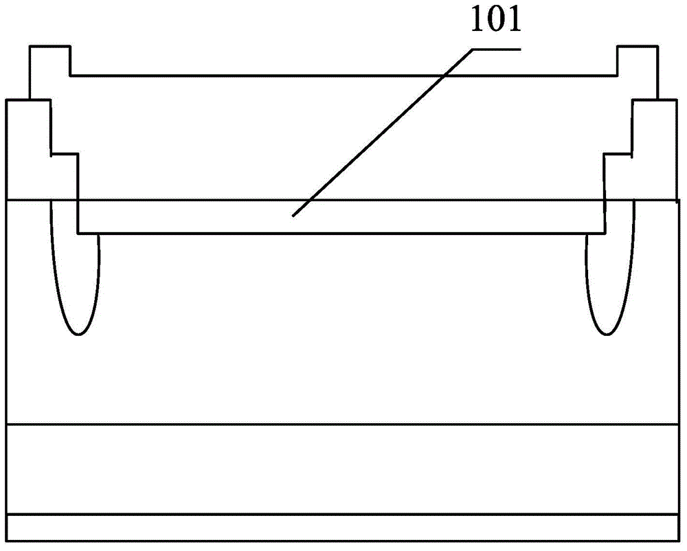
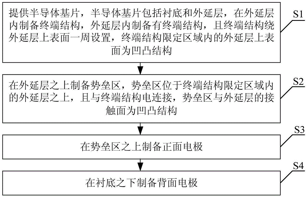
[0049] figure 2 A schematic flowchart of a method for fabricating a Schottky diode provided by an embodiment of the present invention. Such as figure 2 As shown, the manufacturing method of the Schottky diode provided by the embodiment of the present invention includes the following steps:

[0050] Step S1. Provide a semiconductor substrate. The semiconductor substra...


PUM


Abstract

The invention discloses a Schottky diode manufacturing method, which belongs to the technical field of semiconductors. The method comprises the following steps: a semiconductor substrate is provided, wherein the semiconductor substrate comprises a substrate and an epitaxial layer, a terminal structure is manufactured in the epitaxial layer, the terminal structure surrounds the upper surface of the epitaxial layer, and the upper surface of the epitaxial layer in a region limited by the terminal structure has a concave-convex structure; a barrier region is manufactured on the epitaxial layer, wherein the barrier region is located on the epitaxial layer in the region limited by the terminal structure and is electrically connected with the terminal structure, and the contact surface between the barrier region and the epitaxial layer has a concave-convex structure; a positive electrode is manufactured above the barrier region; and a back electrode is manufactured below the substrate. According to the Schottky diode manufacturing method, the surface of the barrier region is manufactured to have a concave-convex structure, forward conduction voltage drop of the Schottky diode is reduced, the manufacturing process is simple, and the cost is low.

Description

technical field [0001] The invention relates to the technical field of semiconductors, in particular to a method for manufacturing a Schottky diode. Background technique [0002] With the development of Schottky diodes, the market demand for them is to lower and lower the forward voltage drop. Such as figure 1 As shown, in the traditional Schottky diode manufacturing method, the surface of the barrier region 101 of the manufactured Schottky diode is a planar structure. Since the surface of the barrier region is planar in this structure, the conductive channel is only a planar structure , the area of ​​the potential barrier region is limited, thereby limiting the current conduction capability of the die per unit area, and greatly limiting the reduction of the forward conduction voltage drop of the Schottky diode. Contents of the invention [0003] The present invention is completed in order to solve the above-mentioned deficiencies in the prior art. The purpose of the pre...

Claims


Application Information

Patent Timeline
Patent Type & Authority Applications(China)
IPC IPC(8): H01L21/329
Inventor 吴志伟黄璇孙海刚
Owner WUXI CHINA RESOURCES HUAJING MICROELECTRONICS
Why Eureka
Try Eureka